







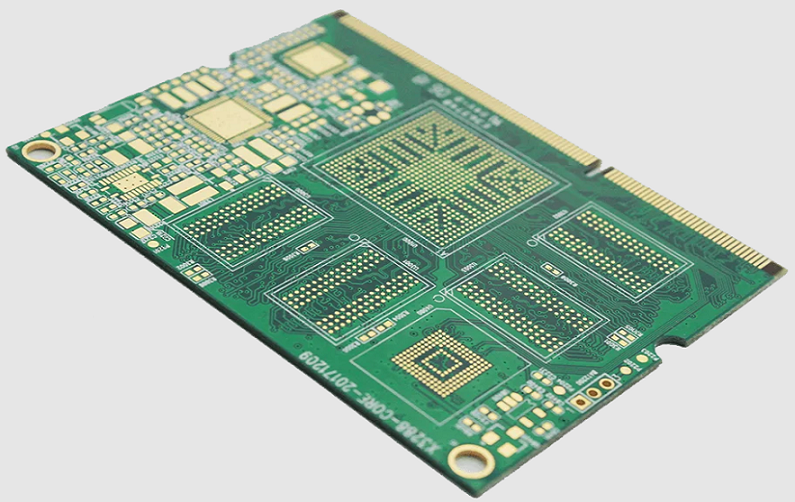
A PCB prototype is an early production version of a printed circuit board used to verify electrical performance, mechanical integration, assembly process, and product reliability before mass manufacturing. A professional pcb prototype process combines schematic review, PCB layout analysis, fabrication, prototype assembly, testing, and engineering validation. Compared with production PCB manufacturing, prototypes focus on rapid design verification, low quantity builds, and fast design iteration.
A reliable prototype circuit board allows engineers to identify issues such as signal integrity problems, incorrect component footprints, thermal limitations, impedance variation, solder defects, and mechanical conflicts before expensive production tooling begins. Depending on complexity, a pcb prototype may range from a simple 2-layer FR-4 board to a high-density HDI pcb prototype with microvias, controlled impedance, and multiple sequential laminations.
A complete prototype process normally includes:
- Design file review and DFM analysis
- Material and stack-up confirmation
- PCB fabrication
- Prototype assembly
- Electrical testing
- Functional validation
- Engineering improvement before production release
For high-speed electronics, semiconductor equipment, automotive systems, and medical devices, a well-controlled prototype stage significantly reduces production risk and improves final product reliability.
What Is a PCB Prototype?
Purpose of Prototype Circuit Boards
A prototype circuit board is manufactured to test whether the electronic design works correctly before moving into volume production.
The main objectives include:
- Electrical performance verification
- Component compatibility confirmation
- Mechanical fit testing
- Firmware and hardware interaction validation
- Manufacturing process evaluation
A prototype PCB is not only a sample board. From a manufacturing perspective, it is an engineering validation platform that provides information about:
- PCB material selection
- Layer structure performance
- Assembly yield
- Thermal behavior
- Signal quality
- Long-term reliability
For example, a high-speed communication board may require:
- 8–16 copper layers
- 50Ω single-ended impedance
- 90Ω or 100Ω differential impedance
- 75–100 μm trace and spacing
- Back drilling for high-speed signal integrity
Typical PCB Prototype Specifications
Prototype requirements vary depending on product complexity.
Common prototype parameters include:
| Parameter | Typical Range |
|---|---|
| Layer count | 2–20 layers |
| Board thickness | 0.6–3.2 mm |
| Minimum trace/space | 50/50 μm–100/100 μm |
| Mechanical drill size | 0.15–0.30 mm |
| Laser microvia | 0.075–0.15 mm |
| Copper thickness | 18–70 μm |
| Impedance tolerance | ±7%–10% |
| Surface finish | ENIG, HASL, OSP |
| Prototype quantity | 5–100 pieces |
For advanced applications, an HDI pcb prototype may include:
- Blind vias
- Buried vias
- Microvias
- Via-in-pad structures
- Sequential lamination
These structures improve routing density but require tighter manufacturing control.
Prototype vs Production PCB
Key Differences
The purpose of prototype manufacturing and production manufacturing is different.
| Category | PCB Prototype | Production PCB |
|---|---|---|
| Quantity | 5–100 pieces | Thousands to millions |
| Main objective | Design verification | Stable mass production |
| Engineering changes | Frequent | Limited |
| Tooling investment | Low | Higher |
| Lead time | Days to weeks | Weeks to months |
| Process optimization | Flexible | Highly controlled |
A pcb prototype allows engineers to modify:
- Component selection
- PCB layout
- Stack-up structure
- Thermal design
- Mechanical dimensions
Production boards require stable:
- Material supply
- Process parameters
- Inspection standards
- Manufacturing yield
Quick Turn PCB vs Standard Production
A quick turn pcb focuses on speed.
Typical quick turn requirements:
- 24–72 hours for simple 2-layer boards
- 5–10 working days for multilayer prototypes
- 10–20 working days for HDI structures
A fast turn pcb service requires:
- Material availability
- Dedicated engineering review
- Fast CAM processing
- Priority production scheduling
However, extremely short lead times may require simplified designs. Complex HDI structures with microvias, thick copper, or special materials require additional process time.
Prototype Manufacturing Process
Design Review and DFM Analysis
The prototype manufacturing process begins with engineering review.
Typical input files include:
- Gerber files
- ODB++ files
- Drill files
- Bill of Materials (BOM)
- Pick-and-place files
- Assembly drawings
Manufacturing engineers evaluate:
- Minimum trace width
- Hole aspect ratio
- Copper balance
- Impedance requirements
- Component spacing
- Solder mask clearance
Typical DFM checks include:
- Minimum annular ring: 0.075–0.10 mm
- Minimum solder mask expansion: 0.05–0.10 mm
- Hole-to-copper clearance: based on layer design
- Controlled impedance calculation before fabrication
Following IPC-2221 design principles helps ensure manufacturability and reliability.
PCB Fabrication Steps
A standard prototype fabrication flow includes:
- Material cutting
- Inner layer imaging
- Inner layer etching
- Layer lamination
- Drilling
- Copper plating
- Outer layer imaging
- Solder mask coating
- Surface finishing
- Electrical testing
- Profiling
For multilayer prototypes:
- Prepreg thickness is controlled during lamination
- Copper thickness is monitored after plating
- Registration accuracy is typically controlled within ±75 μm
For HDI pcb prototype manufacturing:
Additional processes may include:
- Laser drilling
- Microvia filling
- Sequential lamination
- Via-in-pad processing
Prototype Assembly
SMT Prototype Assembly
Surface Mount Technology (SMT) is the most common prototype assembly method.
The process includes:
- Solder paste printing
- SPI inspection
- Component placement
- Reflow soldering
- AOI inspection
Typical SMT parameters:
- Stencil thickness: 0.08–0.15 mm
- Placement accuracy: ±25–50 μm
- Reflow peak temperature: 235–250°C
- BGA pitch: 0.35–1.0 mm
For fine-pitch components:
- X-ray inspection may be required
- Via-in-pad structures may improve routing density
- Microvia technology may be required
Through-Hole Prototype Assembly
Through-hole technology remains important for:
- Connectors
- Power components
- Mechanical parts
- High-current devices
Typical processes:
- Component insertion
- Wave soldering
- Selective soldering
- Manual solder repair
Compared with SMT:
| Technology | Advantage | Limitation |
|---|---|---|
| Surface Mount Technology (SMT) | High density, small components, automated placement | Requires accurate placement and solder process control |
| Through-Hole Technology (THT) | Strong mechanical connection and high reliability | Requires more PCB space and additional assembly steps |
A mixed SMT and THT assembly process is common in industrial prototypes.
Testing and Validation
Electrical Testing
Prototype testing verifies that the board matches design expectations.
Common testing methods include:
- Flying probe testing
- Fixture testing
- Continuity testing
- Isolation testing
- Boundary scan testing
Typical electrical requirements:
- Open/short detection
- Net connectivity verification
- Resistance measurement
- Insulation resistance testing
Functional Validation
Functional testing evaluates real operating conditions.
Engineers may test:
- Power stability
- Signal integrity
- Thermal performance
- Communication interfaces
- Firmware operation
For high-speed boards:
Testing may include:
- Eye diagram analysis
- TDR impedance measurement
- PCIe validation
- DDR signal evaluation
Quality control commonly follows:
- IPC-A-600 acceptance criteria
- IPC-A-610 assembly requirements
- IPC-6012 rigid PCB qualification requirements
Common Design Errors
Incorrect Stack-Up Selection
One common prototype failure occurs when the PCB stack-up is selected without considering:
- Signal frequency
- Copper thickness
- Dielectric thickness
- Material Dk value
- Impedance requirements
For example, a 50Ω RF design may fail if the dielectric thickness changes from the original simulation.
Insufficient Manufacturing Margin
Typical design problems include:
- Trace width below fabrication capability
- Small annular rings
- Excessive via aspect ratio
- Insufficient solder mask clearance
- Components placed too close together
For reliable prototypes:
- Maintain practical spacing
- Confirm material availability
- Review DFM before ordering
Ignoring Assembly Requirements
PCB layout must consider assembly.
Common mistakes:
- No fiducial marks
- Incorrect footprint dimensions
- Missing polarity indicators
- Poor thermal pad design
- Unsupported flex areas
These issues increase prototype debugging time.
Factory Case Study: 12-Layer Communication Prototype
A customer developed a high-speed communication controller requiring:
- 12-layer PCB prototype
- FR-4 high-Tg material
- 1.6 mm board thickness
- 2.5/2.5 mil trace and spacing
- 50Ω impedance control
- 100Ω differential pairs
- ENIG surface finish
- BGA package with 0.5 mm pitch
Initial Problems
The first engineering build showed:
- Differential impedance deviation of approximately 12%
- Excessive via stub impact
- BGA escape routing difficulty
- Minor solder voids after assembly
Manufacturing Improvements
The engineering team implemented:
- Updated stack-up simulation
- Back drilling for high-speed vias
- Improved solder paste aperture design
- Optimized BGA fanout routing
- Adjusted reflow profile
Final Result
After improvement:
- Impedance variation reduced within ±7%
- Assembly yield increased from 94% to 99%
- Signal quality passed validation testing
- Prototype design moved successfully into production preparation
FAQ
What is a PCB prototype used for?
Answer: A PCB prototype is used to verify electrical design, mechanical integration, assembly performance, and product reliability before mass production. It allows engineers to correct design issues at a lower cost.
How long does PCB prototype manufacturing take?
Answer: Simple prototypes may be completed within 3–5 working days, while multilayer and HDI pcb prototype projects commonly require 10–20 working days depending on materials, layer count, and process complexity.
What files are required for a PCB prototype order?
Answer: Typical files include Gerber or ODB++ design files, drill files, BOM, pick-and-place data, assembly drawings, stack-up requirements, and testing specifications.
What is the difference between a PCB prototype and a production PCB?
Answer: A PCB prototype focuses on design validation and engineering improvement, while a production PCB focuses on repeatability, cost control, and high-volume manufacturing stability.

![Understanding PCB Costs & Pricing [Your Complete Guide]](https://hdicircuitboard.com/wp-content/uploads/elementor/thumbs/Understanding-PCB-Costs-Pricing-Your-Complete-Guide-qzzhe6mcaxuolkux3xalfktgavumi9y1aqfbs9bpv4.webp "Understanding PCB Costs & Pricing [Your Complete Guide]")