
Power integrity (PI) and power distribution network (PDN) design are critical for high speed pcb reliability, as unstable power delivery causes signal distortion, EMI, and component failure. This guide details actionable design principles, precise production parameters, and factory-proven practices tailored to hdi pcb, Low Loss PCB, and ultra low loss pcb applications.
Learn more about: What Is High-Speed PCB? A Comprehensive Guide
Power Integrity for High Speed PCB: Core Concepts
Definition & Critical Thresholds
- Power integrity refers to maintaining stable voltage (±2–5% tolerance) and low noise (<100mV) across the PDN for signals ≥1Gbps.
- High-speed designs demand PDN impedance ≤0.1Ω at 100MHz (IPC-2221 standard) to support rapid current switching (≥1A/ns).
- PI directly impacts signal integrity: voltage ripple >5% increases jitter by 30% in 25Gbps high speed pcb designs.
Material Impact on PI
- Low Loss PCB (Df=0.004–0.009 @10GHz) reduces dielectric loss by 25% vs. standard FR-4, stabilizing PDN impedance.
- ultra low loss pcb (e.g., Rogers RO4350B, Df=0.0037 @10GHz) minimizes power plane noise in 50Gbps+ applications.
- hdi pcb requires materials with low CTE (X/Y ≤16ppm/°C) to prevent power plane separation during sequential lamination.
PDN for High Speed PCB: Architecture & Components
PDN Structure Overview
- PDN includes voltage regulator modules (VRMs), bulk capacitors (100µF–1000µF), ceramic decoupling capacitors (0.1µF–10µF), power/ground planes, and vias.
- For high speed pcb, PDN must cover DC to 1GHz frequency range (matching signal edge rates ≥1V/ns).
- hdi pcb PDN uses 1+N+1 stackup with adjacent power/ground planes (spacing ≤0.2mm) to leverage inherent capacitance.
Key PDN Performance Metrics
- Target impedance (Ztarget) calculation: Ztarget = (Vcc × Ripple%) / (0.5 × Imax) — e.g., 3.3V, 3% ripple, 3A Imax = 0.066Ω.
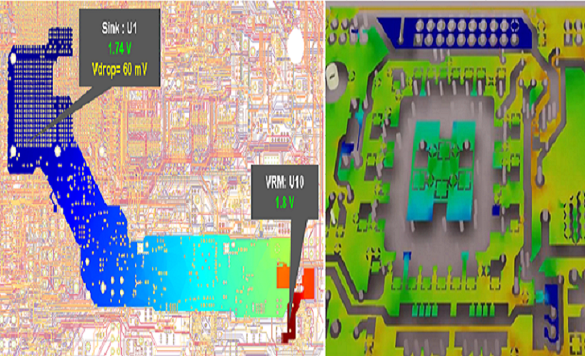
- Voltage drop (IR drop) ≤50mV for high-current traces (≥5A) per IPC-6012 Class 3.
- Plane capacitance: 32.7pF/in² for FR-4 (0.2mm plane spacing) to suppress high-frequency noise.
Principles of PI & PDN Design
Target Impedance: Foundation of PI
- Calculate Ztarget using signal rise time (Tr): Fm = 0.5/Tr (e.g., Tr=1ns → Fm=500MHz, Ztarget=0.048Ω for 1.2V/1A).
- Maintain Ztarget across DC to 1GHz: bulk capacitors cover 1kHz–100kHz, ceramic capacitors 100kHz–100MHz, plane capacitance >100MHz.
- Tolerance: Ztarget ±10% to account for manufacturing variations (e.g., trace width ±0.5mil).
Decoupling Strategy: Noise Suppression
- Bulk capacitors (1000µF, ESR=0.05Ω): placed within 5cm of VRMs to stabilize low-frequency (1kHz–10kHz) PDN.
- Ceramic decoupling capacitors (0.1µF, 0402 package): placed ≤2mm from IC power pins (ESL ≤1nH) for 100kHz–100MHz noise.
- Capacitor array: combine 0.001µF, 0.01µF, and 0.1µF capacitors to cover 1MHz–1GHz frequency range.
Plane Capacitance & Via Optimization
Power/Ground Plane Design
- Plane dimensions: power planes ≤20x dielectric thickness smaller than ground planes (20H rule) to reduce fringing fields.
- Plane spacing: 0.1–0.2mm for high speed pcb (maximizes capacitance while minimizing inductance).
- Avoid plane splits; use stitching capacitors (10nF–100nF) if splits are unavoidable (placement ≤100mil from signal path).
Via Optimization for PI
- Power vias: 0.3mm diameter, 1mm pitch, with anti-pad diameter = via diameter + 0.2mm (IPC-6016).
- Stitching vias (1mm pitch) connect split planes, reducing loop inductance by 60% in hdi pcb.
- Via-in-pad (VIPPO) with epoxy fill: eliminates stub inductance (≤5nH) in 25Gbps+ high speed pcb designs.
Steps for Effective PDN Design
Define Requirements
- Document Vcc (e.g., 1.2V/3.3V), Imax (max current), ripple tolerance (2–5%), and signal rise time (Tr ≥1V/ns).
- Map frequency range: DC to Fm = 0.5/Tr (e.g., Tr=0.5ns → Fm=1GHz) to select decoupling components.
- Align with hdi pcb manufacturing constraints (e.g., microvia diameter ≥0.1mm).
Stackup Design
- High speed pcb: 8-layer stackup (Signal-GND-Power-Signal-Signal-Power-GND-Signal) with 0.15mm dielectric between power/ground planes.
- Low Loss PCB stackup: place power planes adjacent to signal layers to reduce crosstalk by 30%.
- ultra low loss pcb: use symmetric stackup (e.g., 12-layer 4+4+4) to prevent warpage (≤0.3mm/m).
Learn more about : HDI PCB Stack Design: 1+N+1, 2+N+2, 3+N+3, 4+N+4 Explained
Component Placement
- VRMs placed within 3cm of high-current ICs (e.g., FPGAs) to minimize trace inductance (≤5nH).
- Decoupling capacitors: 0.1µF placed ≤2mm from IC power pins, 10µF within 5mm for bulk decoupling.
- For hdi pcb, group decoupling capacitors in BGA fanout regions (0.5mm pitch) to reduce via inductance.
Simulation & Validation
Mandatory PI Simulations
- PDN impedance simulation (using SIwave/HyperLynx) to verify Ztarget ≤0.1Ω across DC–1GHz.
- Voltage drop simulation: IR drop ≤50mV for high-current traces (width ≥8mil for 5A).
- Noise simulation: validate power plane noise <100mV (CISPR 22 Class B).
Physical Validation
- TDR testing of power planes to measure impedance (tolerance ±10% per IPC-TM-650 2.5.5.12).
- Thermal cycling (1000 cycles, -40°C~125°C) to confirm PDN stability (no layer separation).
- Prototype testing with current probes to measure ripple and transient response.
Common PI Pitfalls
Excessive Via Inductance
- Cause: Large via diameter (≥0.5mm) or sparse stitching vias (pitch >5mm).
- Impact: Adds 10nH inductance per via, increasing PDN impedance by 20% in 10Gbps designs.
- Fix: Use 0.2mm diameter vias with 1mm stitching pitch; VIPPO for hdi pcb.
Inadequate Decoupling
- Cause: Using single capacitor value (e.g., only 0.1µF) or placement >5mm from IC pins.
- Impact: Voltage ripple >10% at 100MHz, leading to bit errors in 25Gbps signals.
- Fix: Capacitor array (0.001µF + 0.01µF + 0.1µF) placed ≤2mm from pins.
Narrow Power Traces
- Cause: Trace width <8mil for 5A current (violates IPC-2221).
- Impact: IR drop >100mV, overheating (≥85°C) in high speed pcb.
- Fix: Trace width = 1.2mil/A (e.g., 5A = 6mil; 10A = 12mil) with 2oz copper.
Key Comparisons
| Decoupling Strategy | Frequency Range | PI Improvement | Cost Impact |
|---|---|---|---|
| Single 0.1µF Capacitor | 1MHz–10MHz | 20% noise reduction | Low (+0%) |
| Capacitor Array (0.001µF+0.01µF+0.1µF) | 1MHz–1GHz | 65% noise reduction | Medium (+15%) |
| VIPPO + Capacitor Array | 1MHz–1GHz | 80% noise reduction | High (+30%) |
| Plane Configuration | PDN Impedance | Best For |
|---|---|---|
| Adjacent Power/Ground Planes (0.2mm) | 0.08Ω @100MHz | High speed pcb (10–25Gbps) |
| Split Power Planes + Stitching Caps | 0.2Ω @100MHz | Low-speed non-critical designs |
| Embedded Capacitance Material | 0.05Ω @100MHz | ultra low loss pcb (≥25Gbps) |
Factory Case Study: 16-Layer HDI Ultra Low Loss PCB
Project Specifications
- Layers: 16 (4+8+4 stackup), data rate: 50Gbps (NRZ), material: Rogers RO4350B (Df=0.0037 @10GHz).
- PDN: Vcc=1.8V, Ztarget=0.048Ω, Imax=2A, hdi pcb with stacked microvias (0.12mm diameter).
Issues Encountered
- Voltage ripple (180mV) exceeding 5% tolerance due to inadequate decoupling.
- PDN impedance (0.18Ω @100MHz) above Ztarget, causing signal jitter (50ps).
- IR drop (80mV) in high-current traces (4A) from narrow trace width (6mil).
Improvements Implemented
- Added capacitor array (0.001µF + 0.01µF + 0.1µF) placed ≤1.5mm from IC pins.
- Increased stitching via density (0.8mm pitch) and used VIPPO for power vias.
- Widened high-current traces to 10mil (2oz copper) and reduced trace length by 20%.
Results
- Voltage ripple reduced to 75mV (4.2% tolerance), jitter improved to 32ps.
- PDN impedance stabilized at 0.045Ω @100MHz, meeting target.
- IR drop ≤40mV, manufacturing yield: 97.5% (up from 83% initial run).
| Case Study Aspect | Details / Parameters |
|---|---|
| Project Specifications |
• Layers: 16 (4+8+4 stackup) • Data rate: 50Gbps (NRZ) • Material: Rogers RO4350B (Df=0.0037 @10GHz) • PDN: Vcc=1.8V, Ztarget=0.048Ω, Imax=2A • HDI PCB: Stacked microvias (0.12mm diameter) |
| Issues Encountered |
• Voltage ripple (180mV): Exceeded 5% tolerance (inadequate decoupling) • PDN impedance (0.18Ω @100MHz): Above Ztarget (0.048Ω), 50ps jitter • IR drop (80mV): 4A traces with 6mil width (narrow power traces) |
| Improvements Implemented |
• Capacitor array (0.001µF + 0.01µF + 0.1µF) ≤1.5mm from IC pins • Stitching vias (0.8mm pitch) + VIPPO for power vias • High-current traces widened to 10mil (2oz copper), length reduced by 20% |
| Results |
• Voltage ripple: 75mV (4.2% tolerance), jitter improved to 32ps • PDN impedance: 0.045Ω @100MHz (meets Ztarget) • IR drop ≤40mV, manufacturing yield: 97.5% (up from 83%) |
Common Design Errors
- Ignoring Plane Symmetry: Asymmetric stackup in hdi pcb causes power plane warpage (≥0.5mm/m) — requires symmetric layer count (e.g., 12-layer 6+6).
- Overlooking VRM Placement: VRMs >5cm from high-current ICs add 10nH inductance — factory rework requires trace 加宽 (cost +$0.40/board).
- Incorrect Capacitor Selection: Using 0805 package capacitors (ESL=3nH) instead of 0402 (ESL=1nH) increases noise by 40% — requires redesign.
- Plane Splits Without Stitching: Split power planes cause 2x higher PDN impedance — requires 10nF stitching capacitors (placement ≤50mil from split).
Learn more about: High Speed HDI PCB Design Guide
FAQ
Q1: How to calculate target impedance for high speed pcb PDN?
A1: Use Ztarget = (Vcc × Ripple%) / (0.5 × Imax). For example, 1.2V, 2% ripple, 1A Imax = 0.048Ω. For 50Gbps ultra low loss pcb, use 2% ripple for stricter noise control.
Q2: What decoupling capacitor values work best for hdi pcb?
A2: Combine 0.001µF (1GHz+), 0.01µF (100MHz–1GHz), and 0.1µF (10MHz–100MHz) in 0402 packages. Place ≤2mm from IC pins to minimize ESL (≤1nH).
Q3: How to reduce via inductance in high speed pcb PDN?
A3: Use 0.2mm diameter vias, 1mm stitching pitch, and VIPPO with epoxy fill. For hdi pcb, stacked microvias (0.1mm diameter) reduce inductance by 70% vs. through-hole vias.
Q4: What stackup is best for Low Loss PCB PDN?
A4: 8-layer stackup (Signal-GND-Power-Signal-Signal-Power-GND-Signal) with 0.15mm dielectric between power/ground planes. This configuration leverages 32.7pF/in² capacitance for stable PDN impedance.
If you need high speed PCB manufacturing or design support,our engineering team provides free DFM analysis and quotation.


![Understanding PCB Costs & Pricing [Your Complete Guide]](https://hdicircuitboard.com/wp-content/uploads/elementor/thumbs/Understanding-PCB-Costs-Pricing-Your-Complete-Guide-qzzhe6mcaxuolkux3xalfktgavumi9y1aqfbs9bpv4.webp "Understanding PCB Costs & Pricing [Your Complete Guide]")


