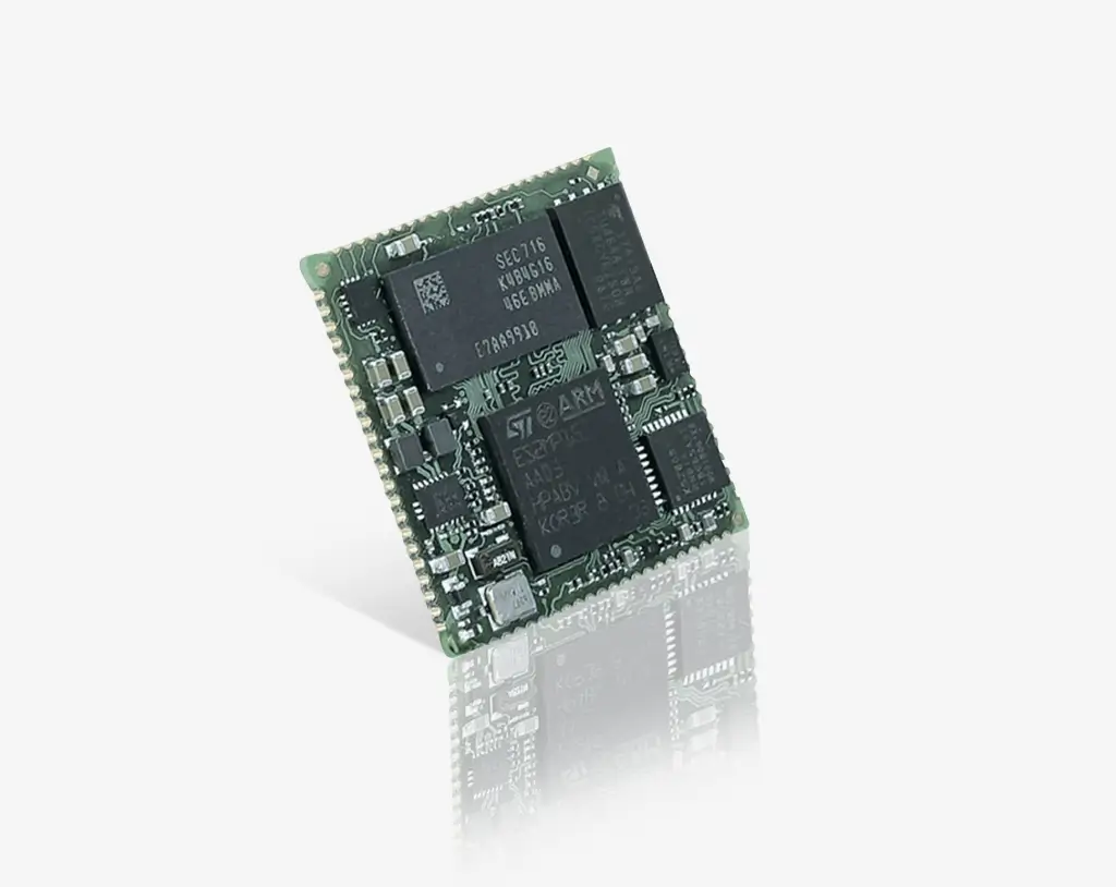
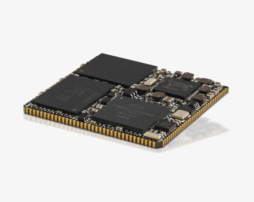
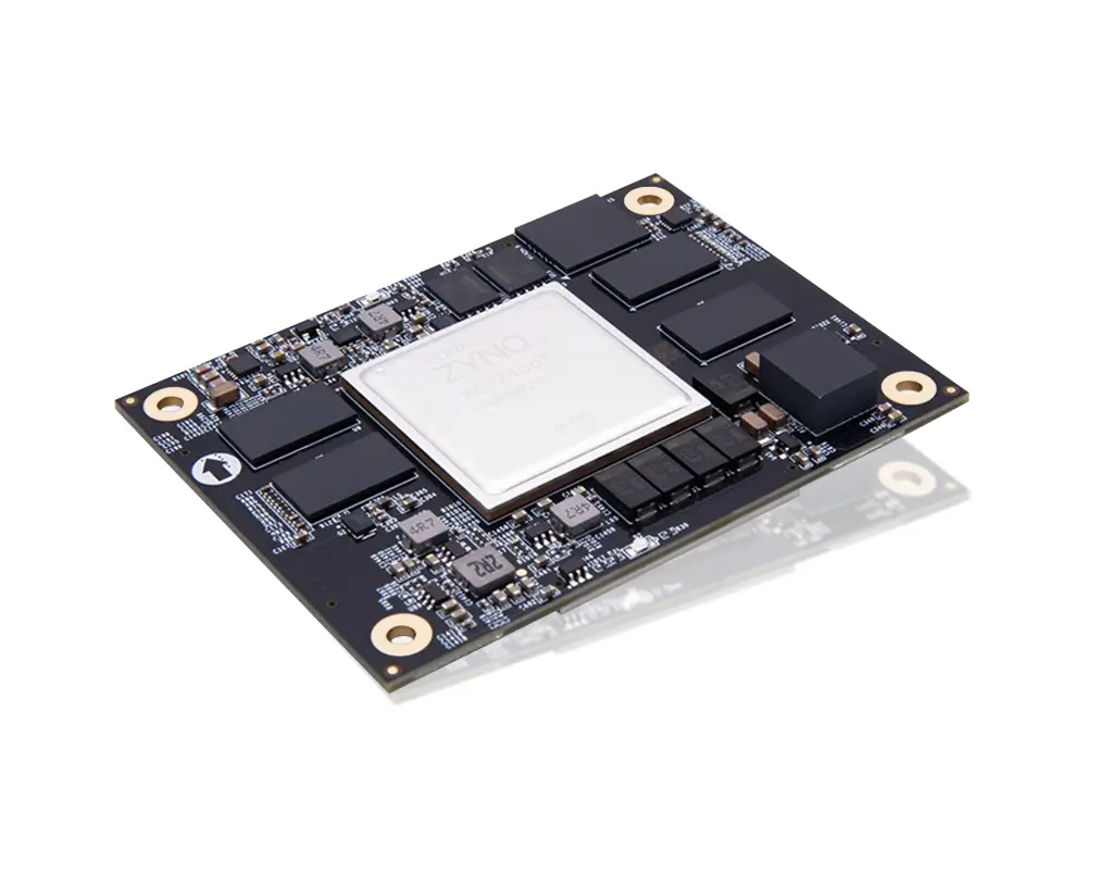
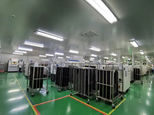
- SMT Assembly, BGA Assembly, Through hole Assembly, Mixed Assembly
- PCB assembly or Box build assembly service delivers a PCBA or a complete electronics assembly in a box
PCB Assembly & PCBA Services | Printed Circuit Assembly Solutions
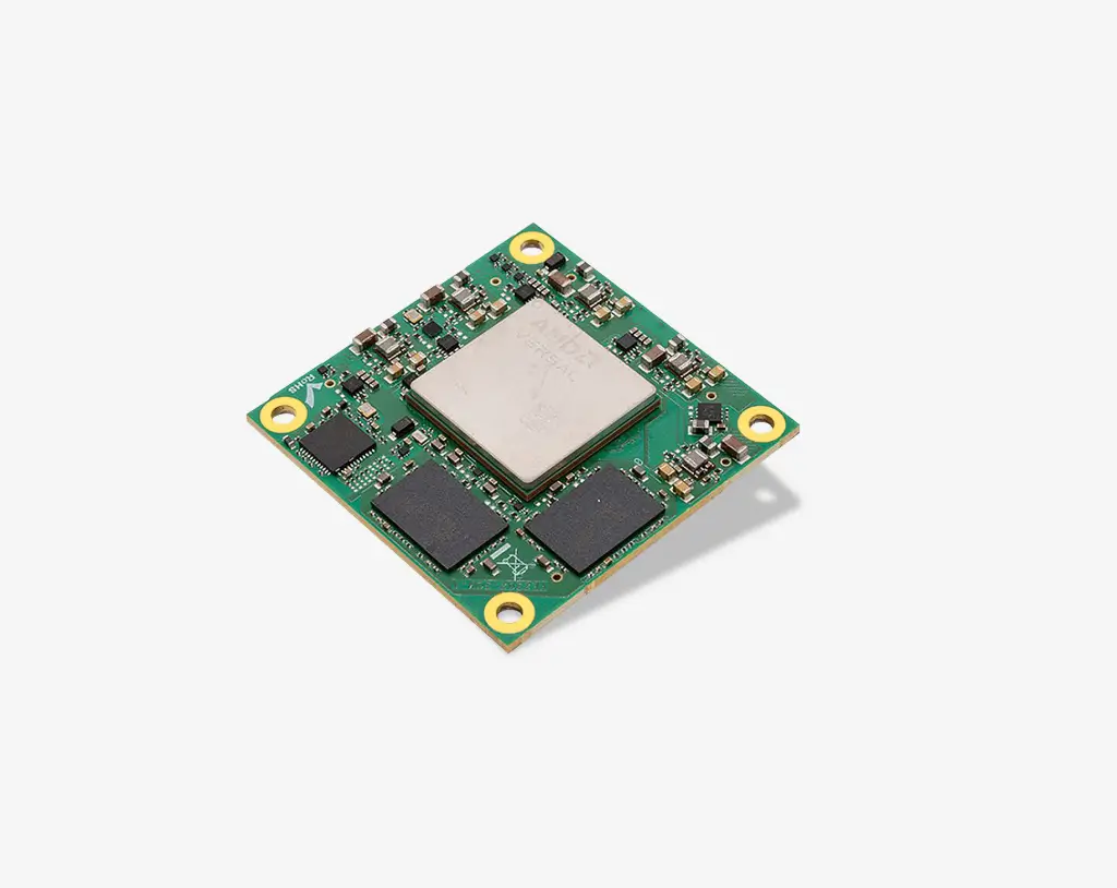
Printed circuit board (PCB) assembly is the process of soldering electronic components onto bare boards. Electronic components installed on the bare board can be through-hole and/or surface mount (SMT). If the assembly has both, it is sometimes referred to as a high mix printed circuit board. PCB assembly is one segment of the electronic manufacturing process. Other segments can include cable/wire harness, mechanical/box builds, programming, and functional testing.
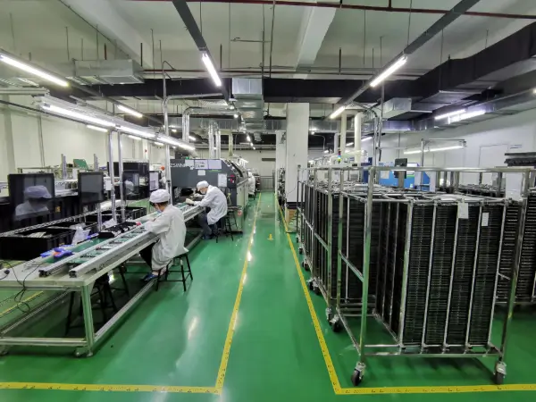
When it comes to reliable PCB assembly and high-precision printed circuit board assembly, our factory delivers end-to-end solutions for every project stage—from prototype PCB assembly to large-scale pcba manufacturing. As a leading PCB assembly manufacturer, we specialize in smt pcb assembly, through-hole assembly, mixed assembly, and conformal coating, with full compliance to IPC-A-610 Class 2/3 and ISO 9001:2015 standards. Whether you need pcb fabrication and assembly for consumer electronics, industrial control panels, medical devices, or automotive systems, our team ensures on-time delivery, 99.8%+ first-pass yield, and tailored support for your unique circuit board assembly needs. We also offer pcb assembly near me and quick-turn prototype printed circuit board assembly (3-day lead time for small batches), making us the trusted partner for startups and Fortune 500 companies alike.
PCB Assembly Types (SMT, Through-Hole & Mixed Assembly)
When selecting PCB assembly solutions, the right assembly type directly impacts product performance, production cost, and long-term reliability. Our factory offers three core circuit board assembly types—SMT, through-hole, and mixed assembly—to match diverse electronics manufacturing needs, with full adherence to IPC-A-610 Class 2/3 standards for commercial and high-reliability applications.SMT PCB Assembly (Surface Mount PCB Assembly)
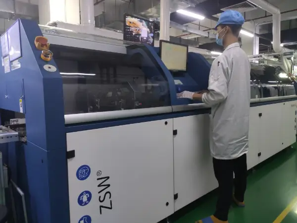
Surface Mount Technology (SMT) has become the backbone of compact, high-performance electronics assembly—our SMT lines are engineered to handle ultra-miniature components, including 01005 passives (0.4mm×0.2mm) and 0.25mm pitch BGAs, perfectly suited for consumer IoT devices, wearable tech, and portable diagnostic medical equipment.- Technical Advantages: Leveraging Juki RX-7R pick-and-place machines, our automated SMT process achieves ±0.03mm placement accuracy—80% higher than manual assembly—while cutting high-volume production lead times by 30%. Automated stencil printing with 3D SPI inspection also reduces material waste by 15%, optimizing cost efficiency.
- User Value: For clients developing miniaturized products (e.g., smart wearables or portable IoT sensors), our SMT assembly shrinks board footprints by 40% without compromising electrical stability, enabling sleeker, more user-friendly product designs that stand out in competitive markets.
- Case Validation: We partnered with a US-based developer of portable glucose monitors to assemble 50,000 PCBs, achieving a 99.8% first-pass yield. The project met FDA 21 CFR Part 820 medical device regulations, with our automated quality checks ensuring consistent performance across all units.
Through-Hole PCB Board Assembly
Through-Hole PCB Assembly is the trusted choice for components demanding exceptional mechanical durability—think power connectors, high-voltage transformers, and industrial control modules that operate in vibration-intensive environments like automotive engines, aerospace systems, and oilfield drilling equipment. Unlike SMT, through-hole components are inserted through precision-drilled board holes and soldered on the reverse side, creating a mechanical bond that resists shock and thermal stress.- Technical Advantages: Each pin delivers 500N of pull force, ensuring superior tensile strength, while the design supports high-power components (up to 200W per part) without compromising connection integrity. Our wave soldering process also ensures uniform solder joints across all through-hole components.
- User Value: For industrial clients operating in harsh conditions (e.g., outdoor industrial controllers or oilfield sensors), our through-hole assembly guarantees 10+ years of reliable operation. This durability reduces post-deployment maintenance costs by 25%, minimizing downtime and extending product lifecycles.
Mixed PCB Assembly (SMT + Through-Hole)
Mixed Technology PCB Assembly merges the precision of SMT for compact signal components with the ruggedness of through-hole for heavy-duty power parts—ideal for complex systems like medical imaging machines, industrial PLCs, and aerospace control panels that demand both miniaturization and durability.- Technical Advantages: We use automated SMT placement for small-signal components (e.g., ICs and resistors) to ensure speed and accuracy, paired with semi-automated through-hole insertion for power-hungry parts (e.g., transformers and connectors). This hybrid approach balances production efficiency with mechanical reliability, adhering to IPC-A-610 Class 3 standards for high-reliability applications.
- User Value: For clients with hybrid component requirements, our one-stop mixed assembly service eliminates the need to coordinate with multiple suppliers. This streamlines your PCB manufacturing and assembly workflow, reducing administrative overhead and cutting overall lead times by 20%—critical for time-sensitive product launches.
PCB Assembly Capabilities & Technical Specs
Our PCB assembly services are backed by industry-leading equipment and strict quality control, enabling high-precision printed circuit board assembly for commercial, industrial, and medical-grade electronics. All processes align with IPC-A-610 Class 2/3 and ISO 9001:2015 standards, ensuring your PCBA circuit board meets performance and regulatory requirements. Below is a breakdown of our core capabilities for PCB board assembly.PCB Assembly Part Procurement Options
A resilient supply chain is the foundation of smooth PCB manufacturing and assembly—our flexible component procurement solutions are designed to eliminate delays and give you greater control over your project:- Full-Turnkey Procurement: We source all active/passive components, ICs, and connectors exclusively through authorized distributors (Digi-Key, Mouser, Arrow) to guarantee authenticity. Every component undergoes 100% counterfeit detection, including X-ray inspection and manufacturer authentication checks. This end-to-end procurement service cuts your project coordination workload by 60%, making it the perfect choice for startups, small businesses, or clients without established supply chain networks.
- Consigned Material: If you already have pre-sourced components, our team manages storage, incoming inspection (including solderability and dimensional checks), and seamless integration into the assembly process. We offer custom labeling and full lot traceability—critical for prototype PCB assembly and aerospace-grade projects requiring strict compliance with AS9100 standards.
- Hybrid Procurement: We specialize in sourcing hard-to-find or obsolete ICs (with 95% success rate for legacy components) while you retain control over proprietary or high-value parts. This balanced approach optimizes cost efficiency and supply chain security, ideal for volume PCB assembly orders with mixed component availability.
SMT & BGA Assembly Specifications
Our SMT PCB assembly line features Juki RX-7R pick-and-place machines and precision reflow ovens, supporting ultra-fine-pitch components for high-density boards. The table below outlines key specs and their user value:- Trust Validation: We delivered 100,000 units of 0.3mm pitch BGA boards for a US automotive client specializing in electric vehicle control systems, achieving 99.85% first-pass yield and meeting IATF 16949 automotive quality standards.
| Technical Parameter | Specification | User Value |
|---|---|---|
| Smallest Component | 01005 passives (0.4mm×0.2mm) | Enables 40% smaller board footprint for IoT/wearable devices |
| BGA Pitch | 0.25mm | Supports high-performance processors for industrial computing/medical devices |
| Placement Accuracy | ±0.03mm (chip components) | Reduces solder defects to <0.05% for high-volume PCBA manufacturing |
| Max Board Size | 500mm×450mm | Accommodates large industrial control panels/automotive PCBs |
Environmental & Compliance Capabilities
For projects with stringent regulatory requirements, our PCB assembly processes adhere to global environmental and safety standards, ensuring market access and long-term reliability:- RoHS/REACH Compliance: All solders, components, and packaging meet RoHS 2.0 (Directive 2011/65/EU) and REACH SVHC (Substances of Very High Concern) requirements, with full documentation provided for global market entry. We also offer leaded solder options for legacy medical or aerospace applications requiring specific material compatibility.
- Conformal Coating: We apply IPC-CC-830 compliant acrylic, urethane, silicone, and parylene coatings to shield assembled PCBs from moisture, dust, chemicals, and thermal stress—perfect for outdoor sensors, industrial equipment, and marine electronics.
- UL Certification Support: Our engineering team provides comprehensive documentation, including material safety data sheets (MSDS) and test reports, to streamline your PCB assembly project’s UL 94V-0 (flame retardancy) and UL 796 (PCB safety) certification process.
Complete PCB Assembly Process (Stencil to Functional Testing)
A standardized, transparent PCB assembly process is the foundation of consistent quality and on-time delivery for your printed circuit board assembly projects. Our 7-step workflow—from stencil preparation to final functional testing—includes real-time quality checks at every stage, supporting prototype PCB assembly and high-volume pcba manufacturing alike.Solder Paste Printing for PCB Assembly
Solder paste printing is the critical first step in smt pcb assembly, directly impacting solder joint integrity. We use automated printers with 3D inspection for precise deposition:- Process Details: Custom laser-cut stencils (0.1mm–0.2mm thickness) are calibrated to pad designs, with ±0.02mm alignment accuracy and 100% SPI (Solder Paste Inspection) for volume/placement verification.
- Prototype Adaptation: 24-hour quick-turn stencil fabrication accelerates prototype printed circuit board assembly time-to-market.
- User Value: Precision printing reduces solder bridging defects by 80% for high-density surface mount pcb assembly projects.
Component Mounting & Reflow Soldering
Post-printing, components are placed and soldered to form your assembled circuit board, with automation ensuring speed and accuracy:- Component Placement: Our machines handle 01005 passives, 0.25mm BGAs, and 50mm connectors (±0.03mm precision), supporting 50,000 components/hour for pcb manufacturing and assembly.
- Reflow Soldering: Custom lead-free/leaded profiles are programmed, with nitrogen inerting to reduce oxidation for medical/aerospace projects.
- Through-Hole Insertion: Semi-automated insertion + wave/selective soldering avoids thermal damage to SMT parts in mixed pcb assy projects.
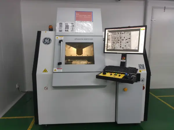
PCB Inspection & Functional Testing
Post-soldering testing validates your circuit board assembly functionality and reliability, with multi-layer defect detection:| Technical Parameter | Specification | User Value |
|---|---|---|
| Smallest Component | 01005 passives (0.4mm×0.2mm) | Enables 40% smaller board footprint for IoT/wearable devices |
| BGA Pitch | 0.25mm | Supports high-performance processors for industrial computing/medical devices |
| Placement Accuracy | ±0.03mm (chip components) | Reduces solder defects to <0.05% for high-volume PCBA manufacturing |
| Max Board Size | 500mm×450mm | Accommodates large industrial control panels/automotive PCBs |
Conformal Coating & PCB Protection Services
For assembled circuit board in harsh environments (outdoor/industrial/marine), conformal coating provides critical protection against moisture, dust, and thermal stress. Our PCB assembly service includes IPC-CC-830 compliant coating solutions, tailored to your product’s operating conditions.Types of Conformal Coating for PCB Assembly
We offer four coating materials, each matched to specific environmental challenges for your printed circuit board assembly:- Acrylic Coating: A cost-effective, fast-curing solution (30 minutes at 60°C) with excellent reworkability—ideal for prototype PCB assembly, consumer electronics, and low-risk indoor devices. It forms a protective barrier that reduces humidity-related failures by 70%, extending product lifespan in controlled environments.
- Urethane Coating: Engineered for chemical and UV resistance, this coating is perfect for automotive electronics, industrial control panels, and outdoor equipment. It delivers 10+ years of reliable protection against harsh elements, cutting long-term maintenance costs by 35% for field-deployed devices.
- Silicone Coating: With a wide operating temperature range (-65°C to 200°C), this flexible coating excels in aerospace systems, medical devices, and industrial equipment exposed to extreme thermal cycling. It resists cracking and peeling, ensuring consistent protection even in rapid temperature fluctuations.
- Parylene Coating: A pinhole-free, ultra-thin coating (down to 0.1μm) that’s biocompatible (ISO 10993) and meets FDA and MIL-STD-883 standards. It’s the top choice for medical implants, military electronics, and precision sensors requiring maximum protection in critical applications.
PCB Protection Process & Quality Control
Our coating workflow integrates with the complete PCB assembly process, with strict checks for consistent coverage:- Masking: Sensitive components (connectors/sensors) are masked to avoid contamination—critical for pcb smt assembly with exposed interfaces.
- Application: Automated spraying (high-volume pcba manufacturing) or selective dispensing (prototypes) ensures ±5μm film thickness accuracy.
- Curing & Inspection: Thermal/UV curing is followed by AOI/adhesion testing (IPC-CC-830) to verify coverage and bond strength.
- Post-Coating Testing: FCT is repeated to confirm assembled circuit board retains electrical performance, with X-ray for BGA defect detection.
Custom PCB Protection Solutions
For unique needs, we offer tailored protection to complement PCB assembly and manufacturing:- Potting/Encapsulation: We use high-performance epoxy or silicone compounds to fully seal PCBs for underwater sensors, high-voltage power supplies, and harsh-environment electronics. This 100% environmental isolation protects against water, dust, and chemical exposure, ensuring reliable operation in submersible or industrial settings.
- Thermal Management Coatings: Heat-dissipating ceramic or graphite-based coatings designed for high-power electronics—including LED drivers, power converters, and industrial inverters. These coatings reduce component temperatures by 15–20°C, preventing overheating and extending the operational life of heat-sensitive components.
Printed Circuit Assembly including
- SMT, Through Hole and Mixed Assembly
- Passive Down to 01005 Sizes
- Ball Grid Array (BGA)
- Ultra-Fine Ball Grid Array (uBGA)
- Quad Flat Pack No-Lead (QFN)
- Quad Flat Package (QFP)
- Plastic Leaded Chip Carrier (PLCC)
- SOIC, Package-On-Package (PoP)
- Small Chip Packages (Pitch of 0.2 mm)
- IC Programming
- Functional Testing
PCB Assembly Capabilities
Download PCB assembly capabilities
To prevent getting it wrong from the start, we have put together our design guidelines, to use as a checklist.
The file lists some of the fabrication features that are typically associated with pcb assembly. The feature limits listed are not comprehensive; Our experienced engineers have also worked with every type of PCB material, so they have the knowledge and expertise to provide recommendations and answer all of your pcb assembly questions. Most importantly, they know how to assist for manufacturability and the potential cost drivers of a project.
| Parts Procurement | Full Turnkey, Partial Turnkey and Kitted/Consigned |
|---|---|
| Assmebly Types | Surface Mount (SMT), Thru-hole, Mixed Technology (SMT/Thru-hole),Single and double sided SMT/PTH , Large parts on both sides, BGA on both sides |
| Largest PCB/Panel Size | 24 x 35ʺ |
| Smallest PCB/Panel Size | 1.2ʺ wide |
| Largest QFP Size/BGA Size | 75 mm x 87 mm |
| BGA Pitch Range | From 0.25 mm to 3 mm |
| Smallest QFP Pitch Range | From 0.25 mm to 3 mm |
| Stencils | Laser cut stainless steel and Nano-coating |
| Components | Passive components smallest size 01005,Fine pitch components smallest size 6 Mils pitch, Leadless chip carriers/ BGA, VFBGA, FPGA & DFN, Connectors and terminals |
| Component packaging | Reels, Cut tape, Tube and Loose parts |
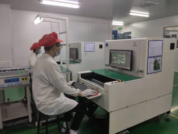
| Inspection | X-ray analysis, AOI and Microscope to 20X |
| Solder Type | Leaded and Lead-free/RoHS compliant |
| Assembly surface mount connectors | Yes |
| Wave Soldering | Yes |
| Conformal Coating And Potting | Yes |
| PCB Finish | SMOBC/HASL, Electrolytic gold , Electroless gold , Electroless silver, Immersion gold, Immersion tin and OSP |
| Panelized PCB | Tab routed ,Breakaway tabs ,V-Scored and Routed+ V scored |
| Design File Format | Gerber RS-274X, 274D, Eagle and AutoCAD’s DXF, DWG BOM (Bill of Materials) and Pick and Place file (XYRS) |
| Other Services | Parts Management, IC Programming and Functional Testing |
View More +
PCB Assembly Types
- Surface Mount (SMT)
- Thru-hole
- Mixed Technology (SMT/Thru-hole)
- Single or Double Sided Placement
PCB Board Assembly Solder Types
- Leaded
- Lead-free/RoHS Compliant
- No-clean and Water Clean Fluxes
PCB Assembly Component Types
- Passive Down to 01005 Sizes
- Ball Grid Array (BGA)
- Quad Flat Package No-Lead (QFN)
- Quad Flat Package (QFP)
- Small Chip Package (Pitch of 0.2 mm)
PCB Assembly Control And Inspection
- AOI Testing
- 3D AOI Testing
- 3D SPI Testing
- X-ray inspection
- In-Circuit Testing
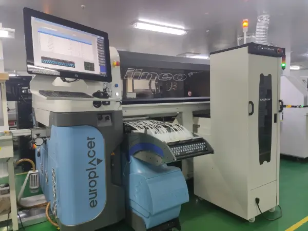
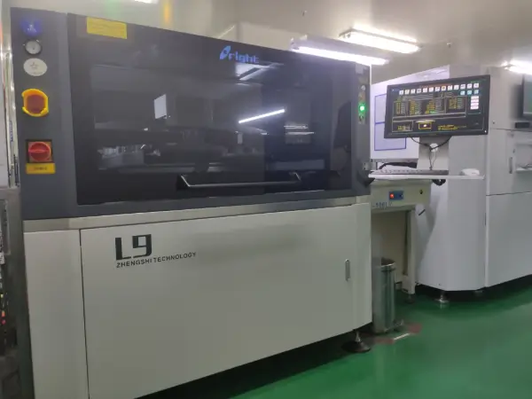
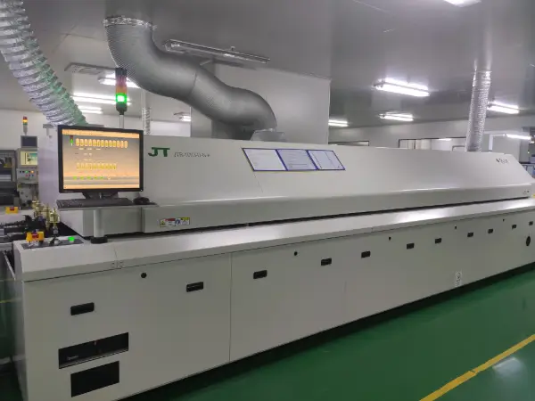
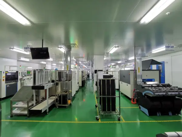
PCB Assembly Manufacturing Equipment
We operate on the principal that quality is built into all of our processes. From beginning to end, quality is in the forefront. We are committed to providing cost-effective, high-quality PCB assembly services with superior customer service.
PCB assembly File Requirements
Please include the following files with your order. Please include then in a single ZIP file.
Gerber Files
Please include all the layers (copper, soldermask, silkscreen, solder paste, etc.
Centroid File
Also known as pick and place file. It should include component locations, rotations and reference designators.
Bill of Materials (BOM) in Excel format. Your BOM should include:
- Reference designators
- Quantity of each part
- Manufacturer part number
- Part description
- Type (SMT, Thru-Hole, Fine-pitch, BGA, etc.).
- Package description (QFN32, SOIC, 0805, etc. package is very helpful but not required).
Printed Circuit Board Assembly Checklist
Benchuang Electronics wants our customers to experience a seamless and accurate assembly process. To ensure that your job is not placed on hold, please follow these guidelines:
Accurate Data
An error free assembly process requires accurate data. Each job should have a BOM (bill of materials), a pick and place file (also known as a centroid file) and matching Gerber data. Add a DO NOT POPULATE (DNP) column to the BOM if there are parts which should not be populated on the PCB.
Ensure Proper Footprints
Some parts are available in different packages. Make sure that the part you specify in the BOM matches the footprint on the PCB.
Organize Components
Parts should be separated into individual bags or trays. Each bag or tray should be marked with Manufacturer name and Manufacturer part number and all reference designators where the part is used. If needed, you can substitute distributor name and part number in place of (or in addition to) manufacturer information.
Multiple Jobs Per Order
The parts for each job should be packaged separately. Include separate BOM and pick and place file for each job
Component Quantities
Include extra parts to account for possible attrition during assembly.
Extra parts will be required on small builds (1 to 25 boards) as follows:
- 0201 to 0603 size: Minimum extra quantity 50 plus required quantity.
- 0805 to 1206 size: Minimum extra quantity 25 plus required quantity.
- On large size components 1 or 2 extra parts is fine.
- We prefer all SMT parts to be on a continuous strip or reel.
- For large runs extra parts by percentage is OK
We will return any unused parts to you when we ship your assembled boards back to you.
Update your BOM and Pick and Place File
If you have any last-minute design changes, please remember to reflect these changes in your BOM, pick and place file and any other relevant documentation.
Mark Polarity
Make sure you indicate proper orientation for all parts that have polarity. Place a dot or a number “1” on pin 1 of ICs where the orientation is not obvious. Ensure that polarized capacitors and diodes are properly marked.
Special Instructions
Provide detailed instructions for any special procedures required to assemble your boards. Include sketches, photos, PDF files and/or drawings as needed.
PCB assembly process overview
After the PCB manufacturing process, where the board structure is completely finalized, the PCB assembly process occurs. During PCB manufacturing, the holes have been pierced to create spaces with specific dimensions for the attachment of designed electric components. Several actions sequentially happen during the assembly phase, with the final aim to enable firm and permanent fixture of the electronic components to the board.
Stencil preparation
The metal sheet should cover the entire surface of the print circuit board except for the holes filled with the solder paste later on. Therefore, the metal sheet must be processed to follow the PCB pattern defined by industrial design, where apertures within the sheet have the same shape, width, and length as their pair holes at the PCB. This metal sheet is widely called a stencil, made of whether brass or stainless steel.
The stencil design is a highly challenging task since the precision of the stencil’s shape and uniformity of stencil thickness are essential for accurate and purposeful PCB assembly. The typical thickness range of a stencil is between 0.0254mm and 0.762mm. The metal sheet thickness is a parameter that depends on the types of electric components used in the particular PCB, and it is determined separately for each printed circuit board. Even the slightest under or oversizing may cause significant issues in later stages of the PCB assembly process. The larger stencil apertures cause so-called balling or bridging. Those phenomena arise during solder application where film covers parts of PCB surface or even whole pathway between two neighbor holes. The result of both cases is an open electric circuit that leaves PCB completely unfunctional. After selecting the required stencil parameters, the metal sheet with specified composition and thickness is ordered from the metal factory, which inspects the sheet’s thickness uniformity using x rays gauge and then ships it to our production plant.
Chemical etching
There are few stencil processing technologies, but laser cutting and chemical etching are the most widely used ones. In the chemical etching process, the metal mask and flexible metal mask are etched from both sides. Firstly, the PCB design should be transferred onto the metal sheet using film. Then, sheets are dipped into the specific acid solution, which enables aperture formation. However, the drawback of this process is that acid interferes with deeper sheet levels, causing undercutting. Therefore, the walls must be additionally polished to form a smooth surface suitable for solder application during PCB assembly. There are two options for wall smoothening: electropolishing which presents a micro etching process, and nickel plating. Electropolishing is a reverse process of electroplating. The electricity is utilized to dissolve excessive metal parts into an electrolyte solution which is swept after processing. Conversely, during the nickel plating, the additional metal layer is applied to walls of apertures whose diameters consequently become reduced.
Laser cutting PCB
Specialized CNC machines are used for laser cutting PCB purposes during the PCB assembly process. Applied laser beams cut the metal sheet according to the pattern provided by the Gerber file. This file contains all technical specifications of PCB, while integrated custom software reads them and then navigates the laser moves through the cutting process accordingly. Since the metallic bond is outstandingly strong, the fine-tunning of laser parameters is necessary to create smooth metal edges. The following parameters play a crucial role during the laser cutting PCB process: beam spot size, beam focus, cutting speed, and laser power. The laser power must be sufficient at all times to enable rays’ penetration through the sheet surface. A beam spot of 0.0254mm is the most widely used one in the PCB assembly since it is suitable for cutting almost all kinds of shapes and aperture sizes. Regardless of the set parameters’ accuracy, there is a need for additional smoothing of aperture walls using the same techniques as in the chemical etching process, either electropolishing or nickel plating.
Solder paste printing
The unique printer kind is used for solder paste applications during the PCB assembly process. This type of printer is widely called a squeegee blade printer. It got its name from squeegees used to press the solder paste across the stencil surface and inside the PCB holes. They may be made either from metal or polyurethane, depending on the pressure ranges they need to generate. The printer’s internal vision system aligns the stencil vertically over the boards. In addition, the printer uses three fiducials, commonly called global fiducial marks, for the stencil’s highest precision positioning over the board. Namely, the global fiducial mark immediately determines and corrects any eventual PCB misalignment in both the X and Y axes before printing operation and during the printing as well. In that way, the possible displacement of either board or stencil under pressure generated by the squeegee is completely avoided.
Squeegee pressure is a parameter that must be controlled with special attention. Increased pressure may cause multiple issues such as greater paste shear that causes paste spreading over the PCB flat surface and causes so-called bridging and bleeding of solder paste. Since the paste is a highly viscous suspension, it requires significant force to flow. The squeegee pressure must be sufficient to generate the force that overcomes the high friction force between the highly viscous paste and the stencil. Once paste movement is initiated, the paste travels across the width of the printable area in a controlled roll, filling in all stencil apertures while simultaneously being swept from the top side of the stencil surface by squeegee blades. The standard operating pressure range of the squeegee is between 0.13kg and 0.27kg per linear centimeter of the printable area. The moving squeegee must induce inertia under whose influence the paste flows inside the PCB holes. Abrupt but controlled motions of squeegees induce inertia, which is why the speed is another parameter that must be monitored continuously. Since the squeegee’s pressure and speed are directly proportional, the speed must be continuously below the upper constraint value, usually 75mm per second. The higher speeds induce the higher friction force between the blades and stencil, leading to blades’ mechanical failure over time.
The third essential parameter of solder printing is the angle between the squeegees and the stencil. The regularly set angle is 60° for the following reason. It forms an optimal incline, so the paste moves downwards to the PCB holes by gravity. If the angle increases, it can cause scooping of the holder paste out of the stencil apertures and consequently an insufficient amount of solder paste. On the contrary, the blades leave a solder paste residue on the stencil after the squeegee has completed a print when the angle decreases.
A regular printing operation lasts between 15 to 45 seconds per print circuit board. The printing is the longest step in PCB assembly, followed by the separation process in which the stencil is separated from the PCB. Postprint inspection is essential for quality assurance of deposited solder paste layers and their suitability for the following step-surface mounting of electrical components. The quality assurance is usually performed with unique 2D vision systems on the printer or separate 3D systems.
Stencil separation and cleaning
The PCB is separated from the stencil at the end of the printing process. During separation, the solder paste must remain in the PCB holes. The speed of stencil removal is crucial to ensure that the stencil doesn’t withdraw any paste from apertures. The regular linear speed of stencil movement is around 3mm per second. The solder paste can’t fully release from the apertures at higher speeds, causing undesired high edges around the deposits.
After few printing operations, the stencil cleaning ensures that there is no accumulation of the paste particles between the stencil and the PCB. The cleaning operation is comprised of two steps: Firstly, the stencil is swept using cleaning chemicals like isopropyl alcohol. In this step, the area underneath the stencil is cleaned. Then, additional vacuum cleaning occurs where the apertures are cleaned to avoid blocking paste flow to PCB holes.
Quality assurance of stencil and squeegee condition after a printing session
Before quality assurance of mechanical parts, the automated cleaning system removes the solder paste residues altogether, so the operator has a clear view of the entire material surface. Then, the operator proceeds with a visual inspection of stencils and squeegees to check if any mechanical defect arose on both blades and stencils. If the operator notices any damage on squeegees or stencils, he needs to replace a defective part to provide a reliable and efficient printing process.
Solder paste composition, properties, and storage
Composition
Solder paste represents a suspension composed of the metal solder particles dispersed in the flux. The metal solders may be made of various elements, but the most common composition is 99.7% tin and 0.3% copper. The metal particles have a spherical shape, and their size may vary according to the type standards specified in IPC J-STD 005. Lead was commonly used in the formulation back in the day. Nowadays, its usage is abandoned due to international environmental protection regulations since it presents a highly hazardous element for human health and the environment. On the other side, the flux is used as an adhesive that bonds the metal spheres and enables electronic components’ mounting to pads on the board. The flux is a highly viscous material containing 60 to 80% of active ingredients that hold metal particles together and prevent oxidation and corrosion. The large percentage of active ingredients within flux prevents the formation of metal oxides on both the base and filler materials to which it is applied.
Furthermore, the flux makes it possible to solder through-hole pin in paste components by printing solder paste in the holes. By weight, a mixed solder paste commonly consists of 90% metal. However, due to their lower density, the non-metallic ingredients of the flux take up to one early half of the paste volume.
Properties
Solder paste is a non-Newtonian type of fluid, more precisely the pseudo-plastic one, meaning that its resistance to flow significantly drops after applied pressure reaches a specific value. The pseudo-plastic behavior is an essential characteristic of the solder paste that allows successful printing. Namely, due to significant changes in flow resistance, the paste may flow in and out of the stencil apertures during the print stroke, but it remains in PCB holes without slumping when the print stroke is done.
The viscosity is a physical property that determines the fluid’s resistance to flow. Besides the compounds that flux comprises, the greatest influence upon flow resistance has a metal to flux ratio. The increase of the metal compounds significantly increases the overall solder paste viscosity. During the printing operation, the thin solder film between the blade and stencil faces a notable temperature increase that reduces the paste viscosity since it is a consequence of a friction force that arises from applied pressure.
Storage of the solder paste
The appropriate storage of solder paste allows maintenance of its desired properties needed for the highest performance of PCB assembly. The solder paste must be stored in an airtight or hermetic container to prevent metal interaction with oxygen and moisture. The large surface area of sphere-shaped metal particles makes them highly prone to corrosion, which decreases the bonding strength in interaction with electronic components. Another parameter that must be controlled is temperature. The storing temperature should be lower than 8 degrees Celsius, while the 1 degree is the lower temperature limit since flux contain the liquid components that could freeze. The controlled storage conditions reduce the oxidation rate of metal particles, but they also reduce the rate at which the thermosensitive flux active ingredients degrade.
Electrical components' mounting
Once solder paste is applied onto the PCB surface, the mounting of the electrical components is done using a so-called pick and place machine. Before putting the pick and place machine to work, its operation algorithm must be programmed by uploading the bill of materials and component placement list to the Mycronic Mycenter workstation. After programming, the operator supplies pick and place machine with all needed electrical components. Now, this robotic device is ready to begin to operate. During its operation, the accuracy of components placement is the critical parameter that reflects the quality of the PCB assembly process. Like the squeegee blade printer, the pick and place machines use three fiducial points to locate the panel and determine the orientation. The fiducials are optical targets that are etched in the copper layer of every board.
Every component gets its barcode that the machine recognizes while the software sends the information about a particular component position at the board. Besides identifying the component and its place, the device detects its dimension and needed rotation angle for its successful placement. This machine also proceeds with the quality assurance of electrical components since it measures capacitance, resistance, and inductance while carrying it. If the discrepancy between the designed and measured parameters of a particular component is detected, the machine immediately removes that component.
Soldering in curing oven
Once placed at the PCB surface, the electrical components must be permanently fixed to it. The permanent fixture is enabled by soldering of the solder paste that firstly melts and then hardens. During hardening, the spatial orientation of atoms within solder changes, and the consequent transition of solder’s physical properties induce the solder joints’ high tensile strength. The melting process occurs in the curing oven, where PCBs travel through it via a conveyor belt. The heated air flows in the counterflow direction relative to conveyor belt movement. The air with a temperature between 250 and 480 degrees Celsius heats the PCBs via a highly efficient convective heat transfer mechanism. Since paste’s set temperature is reached quickly, the curing process lasts shortly, after which the hardening process occurs. The hardening process also happens in the oven, where the atmospheric air cools down the melted solder and finally hardens it.
Inspection and functional test
After the PCB assembly process, the operators visually inspect the PCB to check whether all parts are positioned correctly. After visual inspection, the PCB is connected to the power supply for functional testing. During this test, the normal circumstances in which the PCB operates are simulated, and if no defects are detected, the board is ready for shipment.
Conformal coating
Conformal coating is an important step to protect components against different environmental influences (like moisture).
Conformal coating is applied to a circuit board to create a barrier between contaminants and the PCB. It also creates an insulating layer reducing crosstalk, leakage current and electrochemical migration in the board. The coating material consists of acrylics, polyurethanes, silicons, epoxy, or a combination of resins.
High Quality PCB Assembly
The PCB assembly process occurs after PCB manufacturing, where the board structure is completely formed according to client requirements. The PCB assembly covers actions from stencil preparation and solder paste printing to SMD parts placement, bonds formation in the curing oven, and final inspection of the PCB functionality. After stencil preparation, the solder paste printing takes place. At this stage, tiny apertures that present mounting spots for electrical components must be filled with exceptional precision. Otherwise, some serious issues such as bridging may occur. The bridges often have a micro size and are not visible to the bare eye. That makes them hardly detectable if state-of-the-art inspection devices are not used. Still, they are the most common issue in the PCB assembly process, leading to short circuits or even component burning up. Thus, we at Benchuang Electronics utilize the latest solder paste printing technology, ensuring that every single printed circuit board operates appropriately at the end of the assembly line.
Another critical part of the PCB assembly process is the positioning of electronic components using the pick and place machine. The conductive lines at the board are very tiny, and they must be aligned with the conductive parts of the electronic components. Hence, the electronic devices must be orientated and posted on the board with the highest precision. We use the most precise three fiducial points optical systems to place the surface mounting devices. Finally, at the end of the PCB assembly line, the firm and stable connection between SMDs and board is achieved in the curing oven. The paste soldering enables the PCBs' longevity and durability, which are our ultimate goals besides the PCBs' highest quality.
Get started with Printed Circuit Assembly
- Box build assembly
- Flex pcb assembly
- Rigid flex assembly
- SMT Assembly, BGA Assembly, Through hole Assembly, Mixed Assembly