- AP 8515R, AP 9111R, AP 8525R, AP 9121R, AP 8535R, AP 9131R, AP 8545R, AP 9141R material
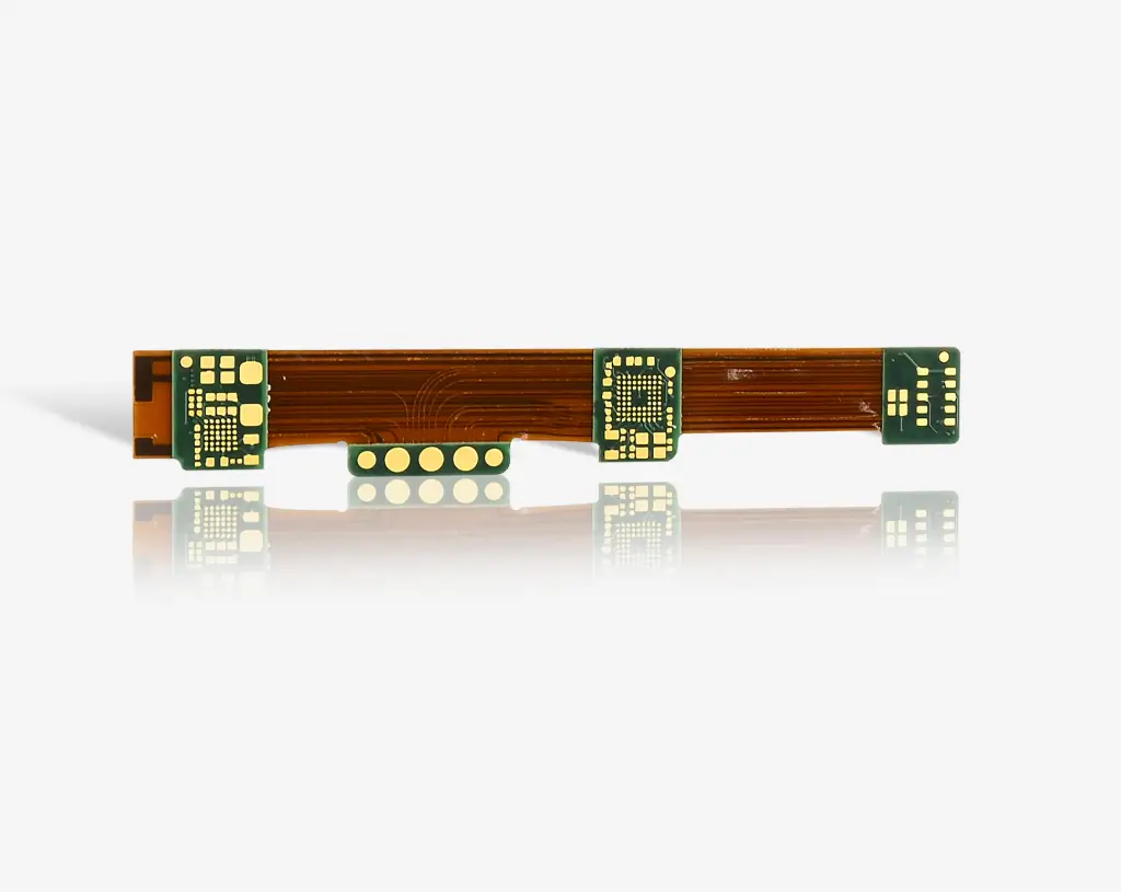
- Rigid Flex circuits are a good solution for both dynamic and static applications. Rigid-Flex can support both plated through hole and micro-via HDI technology.
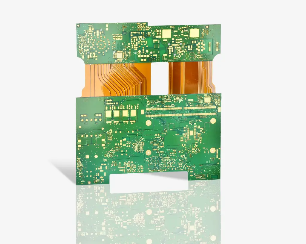
Reliable Rigid Flex PCB Manufacturer | Custom HDI Rigid Flex Circuit Solutions
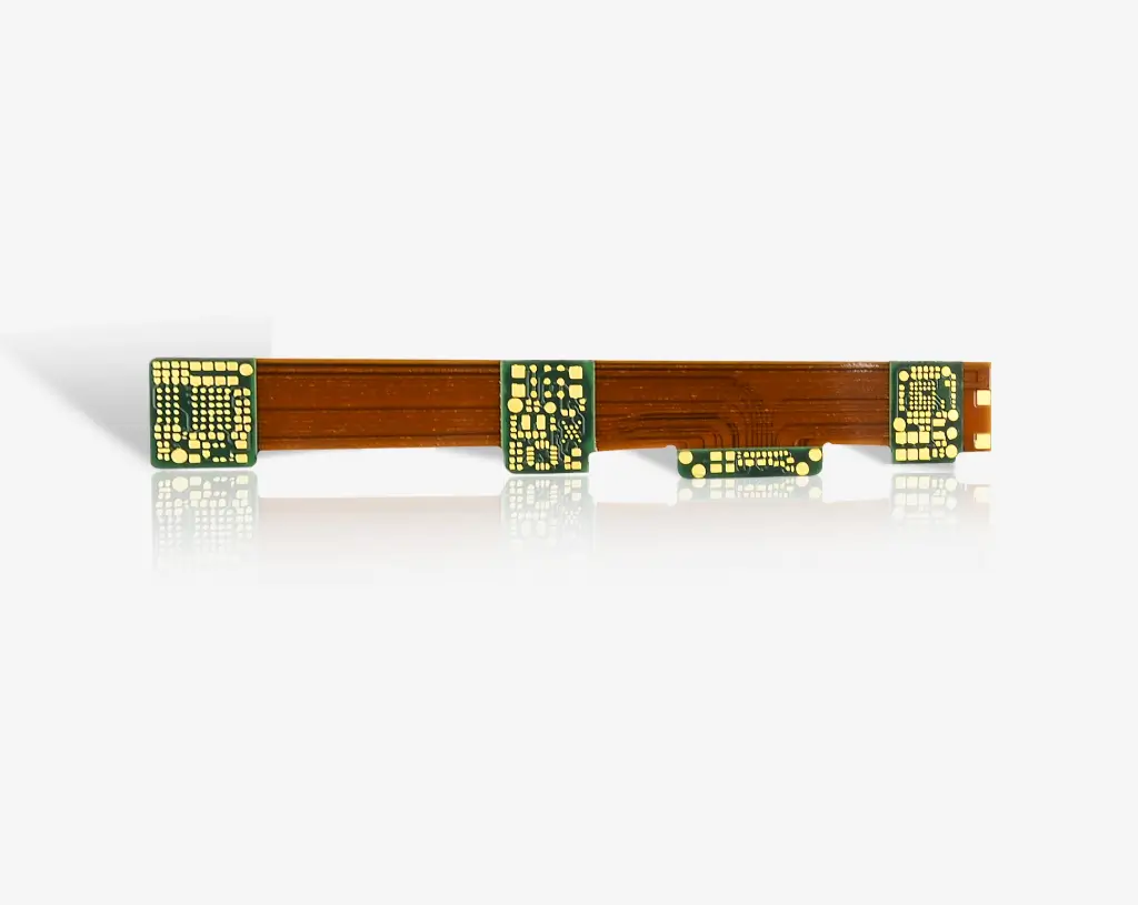
Rigid Flex Board Structures & Layer Configurations
Innovation is driving the demand for smaller, smarter and more versatile devices. Rigid Flex PCB’s, a technology that combines the best of two worlds – the stability of rigid boards and the flexibility of flexible circuits, pun intended! Rigid Flex technology offers a compelling array of advantages, while also posing a set of intriguing challenges.
Rigid flex circuits have been used in the military and aerospace industries for more than 40 years. In rigid flex circuit boards, layers of flexible and rigid materials are used to create both rigid and flexible areas in a single package.
Rigid flex circuits combine the best of both rigid boards and flexible circuits integrated together into one circuit.
As an industry-leading rigid flex PCB manufacturer, we’ve engineered a diverse range of rigid flex board structures and layer configurations to meet the precision demands of high-end electronics across global sectors. Our core structural offerings include:
- Standard Rigid-Flex Structures: Combine 1–2 rigid regions with 1–4 flexible segments, tailored for compact consumer tech like smart wearables. The flexible sections support dynamic bending up to 10,000 cycles while maintaining signal stability, fully compliant with IPC-6013/3 rigid-flex circuit standards. We optimize the rigid-flex transition zone with rounded edges (≥0.5mm radius) to reduce stress concentration during repeated use.
- HDI Rigid Flex Configurations: Integrate laser-drilled micro-vias (minimum diameter 0.1mm) and stacked vias for high-density interconnect needs—ideal for aerospace avionics and medical implant devices. We support 2–12 layer counts, achieving ±0.02mm interlayer alignment via automated optical registration, a critical spec for high-pin-count component integration.
- Asymmetric Rigid-Flex Designs: Customize rigid-to-flexible area ratios to fit asymmetric product housings (e.g., military communication terminals). Flexible hinges are reinforced with extra PI coverlay to withstand extreme vibration, meeting MIL-STD-883H shock resistance requirements (10g acceleration, 10Hz–2000Hz).
All rigid flex PCB structures undergo 3D thermal-mechanical simulation before production, ensuring compatibility with your assembly process and long-term reliability in target environments.
Rigid Flex Circuit Capabilities & Customization Options
Our rigid flex circuits deliver industry-leading performance with fully customizable features, addressing unique project needs for clients in 50+ countries. Key capabilities include:
- Environmental Resistance Tuning: Tailor rigid flex PCBs for extreme conditions—high-temperature solutions (-55℃ to 150℃) for automotive under-hood components (e.g., BMS modules) and IP67-rated moisture-proof designs for marine electronics. All configurations comply with RoHS 3.0 and REACH regulations, with optional flame-retardant materials (UL 94V-0) for enclosed systems.
- Signal Integrity Optimization: For high-frequency applications up to 60GHz, we use low-loss substrates (LCP, PTFE) and precision impedance control (±5% tolerance) to minimize insertion loss (≤0.3dB/inch at 24GHz). This makes them ideal for 5G base station modules and satellite transceivers where signal fidelity is non-negotiable.
- Industry-Specific Customization: As a specialized rigid flex PCB manufacturer, we offer ISO 13485-certified biocompatible materials (USP Class VI) for implantable medical devices, and nickel-copper shielding for military-grade systems to reduce EMI by 40%.
We provide free design consultations to translate your prototype requirements into mass-production-ready solutions, with engineering feedback within 24 hours for urgent projects.
Professional Rigid Flex PCB Design Guidelines & Tips
Our design guidelines are developed by engineers with 15+ years of global project experience, helping you avoid common pitfalls and accelerate time-to-market:
- Flexible Region Design: For dynamic bending, maintain a minimum bend radius of 5x the board thickness—critical for wearables and foldable devices. Avoid placing components within 0.5mm of the rigid-flex transition zone to prevent solder joint cracking, aligning with IPC-2223 design standards. We recommend adding tear-stop notches (radius ≥0.3mm) at flex region edges for extra durability.
- Via Placement Best Practices: Position vias at least 0.3mm away from flexible hinges to avoid stress-induced damage. For high-reliability aerospace projects, use filled-and-capped vias to block moisture ingress and ensure long-term performance in harsh environments.
- Global Design Support: Our engineering team offers free DFM reviews within 24 hours. We validate designs against regional standards (e.g., FCC for telecom, FDA for medical) and mass production feasibility, reducing iteration cycles by 30%.
High-Quality Rigid Flex Board Materials & Substrates
We source premium substrates from top global suppliers (Rogers, DuPont) to ensure consistent performance across all use cases:
- Flexible Substrates: Use 25μm–125μm polyimide (PI) films for high-temperature resistance (-200℃ to 260℃), ideal for automotive and aerospace rigid flex PCBs—all PI materials meet UL 94V-0 flame retardant standards. For cost-sensitive consumer electronics, we offer 50μm–125μm PET substrates with reliable insulation (dielectric strength ≥20kV/mm) and flexibility.
- Rigid Substrates: Integrate FR-4 (FR-406, FR-408) and high-Tg FR-4 (Tg ≥170℃) for rigid regions, supporting SMT and through-hole component assembly. High-Tg variants reduce warpage during reflow soldering, critical for dense component layouts in 5G devices.
- Adhesives & Coverlays: Provide acrylic (for low-temperature applications) and epoxy (for high-reliability projects) adhesives, paired with PI coverlays for enhanced chemical resistance and bending durability. All materials are RoHS 2.0 and REACH compliant, ensuring seamless global market access.
Precision Rigid Flex PCB Fabrication & Manufacturing Steps
Our fabrication process adheres to IPC-A-600 Class 3 standards, delivering aerospace-grade precision for every order:
- Prototype & Pre-Production: Small-batch prototypes (1–50 pcs) are completed in 3–5 working days, with laser drilling (±25μm accuracy) and 100% AOI defect detection. We offer free sample testing (impedance, flex cycle) for critical projects.
- Mass Production Workflow:
- Substrate lamination: Achieve ±0.01mm alignment tolerance via laser registration systems.
- Laser micro-via drilling & copper plating: Ensure via wall thickness ≥12μm for reliable conductivity.
- Solder mask application & coverlay lamination: Use photoimageable solder mask for precise openings (≥0.15mm).
- Final inspection: X-ray testing for hidden via quality, thermal shock testing (-55℃~125℃, 1000 cycles) for reliability validation.
- Global Delivery: As a trusted rigid flex PCB supplier, we offer DHL/FedEx urgent shipping (2–3 days to North America/Europe) and cost-efficient sea freight for bulk orders (10k+ pcs). All shipments include detailed customs documentation (material certificates, compliance reports) to avoid delays.
Static & Dynamic Rigid Flex PCB Application Types
We categorize rigid flex PCBs into static and dynamic types based on bending requirements, each optimized for specific scenarios:
- Static Rigid-Flex PCBs: Designed for one-time or limited bending (e.g., device assembly positioning), widely used in medical ultrasound probes and industrial control panels. Flexible regions are reinforced with 50μm PI coverlay to prevent accidental damage during installation, with a minimum bend radius of 3x the board thickness.
- Dynamic Rigid-Flex PCBs: Engineered for repeated bending (up to 100,000 cycles), ideal for wearable straps, automotive foldable displays, and aerospace deployment mechanisms. We use high-ductility rolled-annealed copper foils (18μm–35μm) and low-modulus adhesives to extend service life, with bend radius optimized to 5x the board thickness for dynamic loads.
Key Rigid Flex PCB Design Best Practices
To maximize the reliability of your rigid flex PCB design, follow these critical best practices:
- Minimize Transition Zone Stress: Add rounded corners (radius ≥0.5mm) at rigid-flex transitions to reduce stress concentration—essential for military-grade and aerospace applications. Avoid sharp edges or right-angle bends in flex regions.
- Component Placement Optimization: Place heavy components (e.g., connectors, capacitors) only on rigid regions, maintaining a 1mm clearance between flexible regions and component leads. This prevents bending-induced solder joint failure in dynamic applications.
- Simulation & Validation: Use finite element analysis (FEA) to test bending fatigue before prototyping. Our engineering team offers free FEA simulation support for high-value projects, identifying potential failure points early in the design cycle.
Core Benefits of Custom Rigid Flex PCBs
Custom rigid flex PCB solutions offer unique advantages over traditional rigid or flexible PCBs:
- Space & Weight Reduction: Integrate multiple rigid boards into a single rigid flex assembly, cutting assembly space by 30–50% and reducing product weight by 20–40%. This is critical for aerospace (satellite payloads) and portable medical devices (wearable monitors).
- Enhanced Reliability: Eliminate inter-board connectors (a common failure point), improving signal integrity and reducing EMI for high-precision systems. Our custom designs achieve a 99.9% first-pass yield in mass production, lowering long-term maintenance costs.
- Streamlined Assembly: Simplify production processes by reducing the number of components and interconnections. This lowers assembly costs by 15–25% and accelerates time-to-market for consumer electronics and automotive projects.
Rigid Flex PCB Applications Across Key Industries
Our rigid flex PCBs serve industries with strict performance and compliance requirements:
- Aerospace & Defense: Used in satellite communication modules and missile guidance systems, meeting MIL-STD-883H (shock, vibration) and AS9100D standards. They withstand extreme temperatures (-55℃~125℃) and vacuum environments, with zero performance degradation during long-term missions.
- Medical Devices: Applied in implantable pacemakers, portable diagnostic tools, and surgical robots. Biocompatible materials (USP Class VI) and ISO 13485 certification ensure patient safety, with designs supporting sterilization (autoclave, gamma radiation).
Automotive & 5G: Deployed in EV battery management systems (BMS) and 5G base station antennas. High-temperature resistance (-40℃~150℃) and high-frequency performance (up to 60GHz) support next-gen electronics, with compliance to AEC-Q200 (automotive) and FCC Part 15 (telecom) standards.
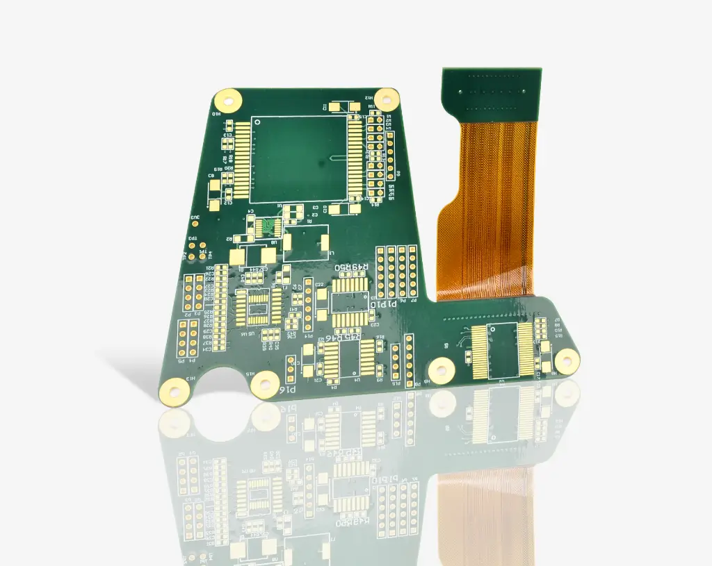
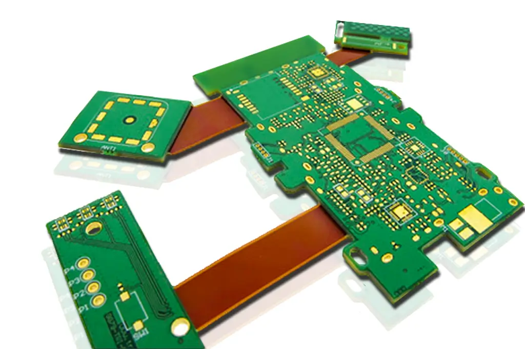
Rigid Flex Board Structures
There are numerous, different structures available. The more common ones are defined below:
Traditional rigid flex construction (IPC-6013 type 4) Multilayer rigid and flexible circuit combination containing three or more layers with plated through holes.
Asymmetrical rigid flex construction, where the FPC is situated on the outer layer of the rigid construction. Containing three or more layers with plated through holes.
Multilayer rigid flex construction with buried / blind via (microvia) as part of the rigid construction. 2 layers of microvia are achievable. Construction may also include two rigid structures as part of a homogeneous build.
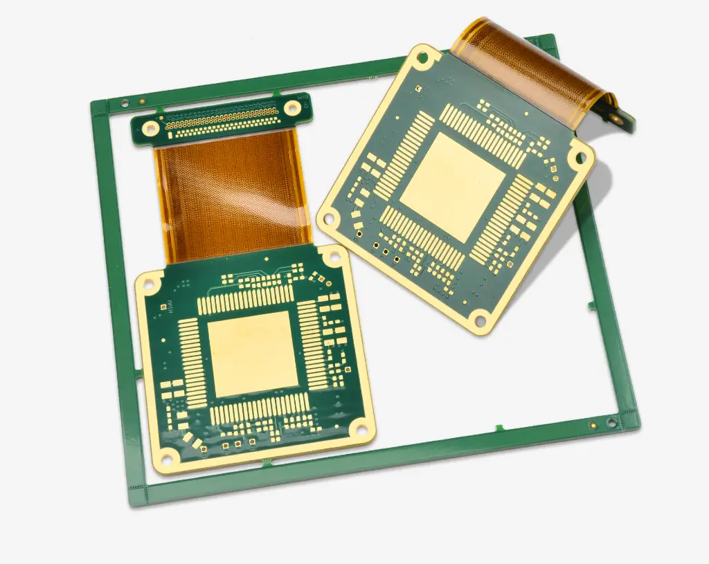
Rigid Flex Circuit Capabilities
Learn about our services, capabilities, and testing for quick turn rigid-flex PCBs. Benchuang Electronics manufactures your rigid flexible circuit boards with full intellectual property protection.
Rigid Flex PCB Design Guidelines
Download our design guidelines for rigid flex PCBs
To prevent getting it wrong from the start, we have put together our design guidelines, to use as a checklist.
The file lists some of the fabrication features that are typically associated with rigid flex. The feature limits listed are not comprehensive; Our experienced engineers have also worked with every type of PCB material, so they have the knowledge and expertise to provide recommendations and answer all of your rigid flex PCB questions. Most importantly, they know how to assist for manufacturability and the potential cost drivers of a project.
| Description | Production | Advanced |
|---|---|---|
| Board Dimensions | ||
| Max. Finish Board Size | 16"X20" | 18"X26" |
| min. Finish Board Size | 0.2"X0.2" | 0.15"X0.15" |
| Max. Board Thickness | 0.250"(+/-10%) | 0.280"(+/-8%) |
| Min. Board Thickness | 0.016"(+/-10%) For 4L | 0.016"(+/-10%) For 4L |
| Lamination | ||
| Layer Count | 2~26L | 30L |
| Layer to Layer Registration | +/-4mils | +/-2mils |
| Drilling | ||
| Min. Drill Size | 6mils | 5mils |
| Min. Hole to Hole Pitch | 16mils(0.5mm) | 18mils(0.35mm) |
| True position Tolerance | +/-3mils | +/-2mils |
| Slot Diameter Tolerance | +/-3mils | +/-2mils |
| Min gap from PTH to track inner layers | 7mils | 6mils |
| Min gap from PTH to the border of rigid flex | 35mils | 30mils |
| Min. PTH Hole edge to PTH Hole edge space | 8mils | 7mils |
| Plating | ||
| Max. Aspect Ratio | 8:1 | 10:1 |
| Cu Thickness in Through hole | >1mils | >1mils |
| Plated hole size tolerance | +/-2mils | +/-1.5mils |
| NPTH hole tolerance | +/-2mils | +/-1mils |
| Via in pad Fill Material | Epoxy resin/Copper paste | Epoxy resin/Copper paste |
| Layer | ||
| Min. Trace/Space | 2.5mils / 2.5mils | 2mils / 2mils |
| Min. pad over drill size | 6mils | 4mils |
| Max. Copper thickness | 1~2 oz | 3 oz |
| Line/ pad to board edge | 6mils | 4mils |
| Min gap from Copper to the border of rigid flex | 10mils | 8mils |
| Line Tolerance | +/-15% | +/-10% |
| Metal Finish | ||
| HASL | 50-1000u'' | 50-1000u'' |
| HASL+Selective Hard gold | Yes | Yes |
| OSP | 8-20u'' | 8-20u'' |
| Selective ENIG+OSP | Yes | Yes |
| ENIG(Nickel/Gold) | 80-200u''/2-9 u'' | 250u''/ 10u'' |
| Immersion Silver | 6-18u'' | 6-18u'' |
| Hard Gold for Tab | 10-80u'' | 10-80u'' |
| Immersion Tin | 30u''min. | 30u'' min. |
| ENEPIG (Ni/Pd/Au) | 125u"/4u"/1u'' min. | 150u"/8u"/2u'' min. |
| Soft Gold (Nickel/ Gold) | 200u''/ 20u''min. | 200u''/ 20u'' |
| Coverlay | ||
| Thickness(Min) (PI / ADH) | 0.5mils / 1mils | 0.5mils / 1mils |
| dam width | 20mils | 15mils |
| registration tolerance | +/-10mils | +/-8mils |
| Solder Mask | ||
| S/M Thickness | 0.4mils min. | 3mils max. |
| Solder dam width | 4mils | 3mils |
| S/M registration tolerance | +/-2.5mils | +/-2mils |
| S/M over line | 3.5mils | 2mils |
| Legend | ||
| Min. Space to SMD pad | 6mils | 4mils |
| Min. Stroke Width | 6mils | 5mils |
| Min. Space to Copper pad | 6mils | 4mils |
| Standard Color | White or Yellow | N/A |
| Electrical Testing | ||
| Max. Test Points | 30000 Points | 30000 Points |
| Smallest SMT Pitch | 20mils | 16mils |
| Smallest BGA Pitch | 20mils | 16mils |
| Laser Rout | ||
| Min. Rout to copper space | 6mils | 4mils |
| Rout tolerance | +/-2mils | +/-2mils |
| NC Rout | ||
| Min. Rout to copper space | 8mils | 4mils |
| Rout tolerance | +/-4mils | +/-3mils |
| Impedance controll | ||
| Impedance controll | +/-8% | +/-5% |
| EMI | ||
| PC-5500&PC-5600 | Yes | Yes |
| Stiffener | ||
| PI | Yes | Yes |
| FR4 | Yes | Yes |
| Metal | Yes | Yes |
| Conductive & thermal adhesive | ||
| 3M Type | Yes | Yes |
| Eccobond | ||
| Eccobond over Flex width | 60mils | 60mils |
View More +
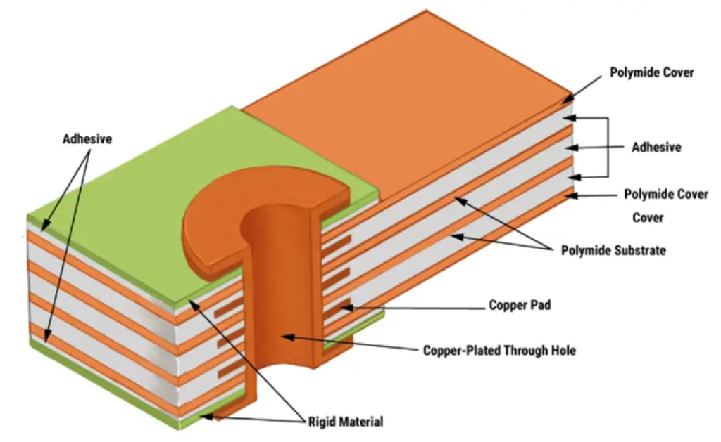
Rigid Flex Board Material
PCB materials used in flex sections are just a few microns thick but can be reliably etched. This often makes them preferable over rigid boards. Flex circuits are built using unreinforced substrates made up of polyimide dielectric film cladded with rolled copper. The rolled copper is more flexible than the copper foil used in the rigid PCBs. Bondply is used to isolate the conducting layers similar to prepreg found in rigid boards. It is a layer of polyimide film with adhesive coated on either side. This layer also insulates the outer surfaces of the flex stackup.
Flex materials offer better dielectric constant compared to standard rigid materials. They offer uniform thickness as they are made of acrylic base. The rigid materials, on the other hand, are built from interwoven glass fiber and the thickness of these materials may not be uniform. Below are few flex materials that we generally use:
| Product | KKapton® Thickness | Copper Thickness |
|---|---|---|
| AP8515 | .001" | 1/2 ounce (.0007") |
| AP9111 | .001" | 1 ounce (.00014") |
| AP9212 | .001" | 2 ounce (.00028") |
| AP8525 | .002" | 1/2 ounce (.0007") |
| AP9121 | .002" | 1 ounce (.00014") |
| AP9222 | .002" | 2 ounce (.00028") |
| AP8535 | .003" | 1/2 ounce (.0007") |
| AP9131 | .003" | 1 ounce (.00014") |
| AP9232 | .003" | 2 ounce (.00028") |
| AP8545 | .004" | 1/2 ounce (.0007") |
| AP9141 | .004" | 1 ounce (.00014") |
| AP9242 | .004" | 2 ounce (.00028") |
| AP8555 | .005" | 1/2 ounce (.0007") |
| AP9151 | .005" | 1 ounce (.00014") |
| AP9252 | .005" | 2 ounce (.00028") |
| AP8565 | .006" | 1/2 ounce (.0007") |
| AP9161 | .006" | 1 ounce (.00014") |
| AP9262 | .006" | 2 ounce (.00028") |
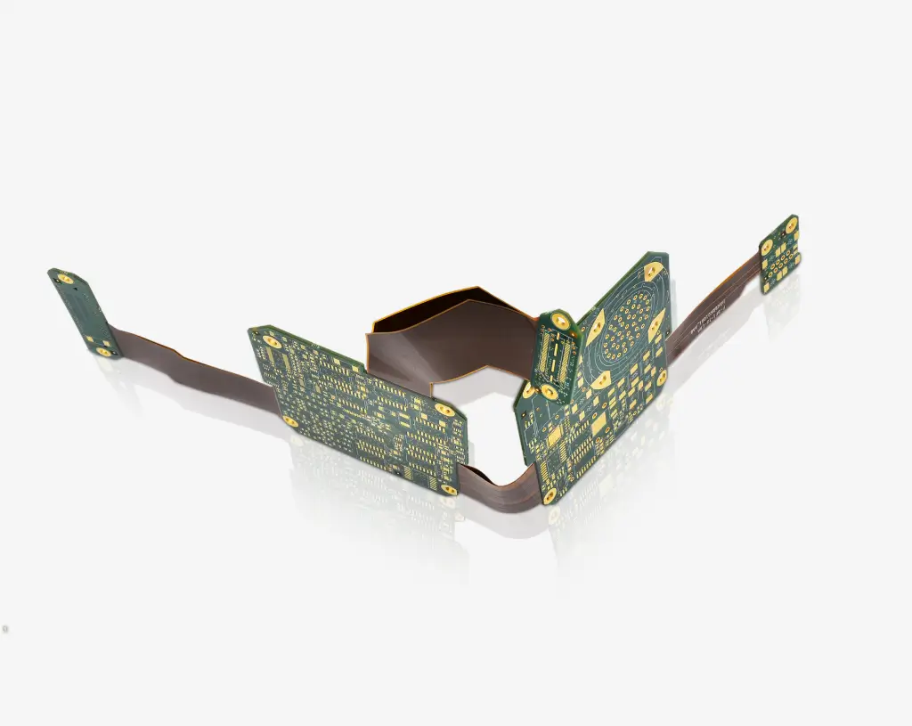
Rigid Flex design
The designs of Rigid-Flex PCBs are a little more complex as these boards are designed in 3D, which allows the board to be folded or twisted to create the desired shape for the product. Designing a board in 3D means they can offer greater spatial efficiency and can subsequently be used in special instances where space and weight reduction may be necessary, such as in medical devices.
Rigid-Flex PCBs are usually thinner than other boards, meaning it’s a great option for any thin or light packaging needs your products may have. With thin copper layers and adhesive-less laminates, it’s a great small, thin and light solution for your circuit design needs.
Flex to install & dynamic flex PCBs
There are two common types of Rigid-Flex PCBs; flex to install and dynamic flex.
Flex to install: this is the most common of the two and applies when a board only folds once, either when the device or product is assembled or dismantled, but is otherwise sturdy and stable throughout.
Dynamic flex: a dynamic flex board will be used when a product is required to fold and bend when in use, meaning they are highly durable and can last through a thousand flex cycles.
Whilst the design might be a touch more complex, and the process slightly more time consuming than the usual printed circuit board, they are an investment worth making with their versatile and durable nature.
Important Rigid Flex PCB Design Guidelines
For all the advantages of rigid-flex PCBs, they also present challenges for PCB designers. Designers must consider not only the electrical aspects of a design but also the mechanical dynamics of the PCB. If you happen to be working on a rigid-flex PCB, following rigid-flex PCB design guidelines will save you from committing costly mistakes.
Avoid Plated Through Holes on the Bending Areas
Avoid placing pads and vias on the bending area of the flex part of a PCB. Areas near the bend line will deliver mechanical stress that could jeopardize the structure of the plated holes.
Pads and vias can be placed on areas that are not subjected to bending, although it’s not recommended. In such cases, use anchors to strengthen the plated holes. Additionally, use a teardrop to connect the trace to the plated hole for stronger joints. It’s also a good practice to use larger pads and vias.
Pay Attention to Routing Across the Bend Area
Traces across the bend line should be kept straight and perpendicular. It’s better to use narrower traces spread evenly across the flexible area. Adding dummy traces can help increase mechanical sturdiness, protecting the traces from breaking. For a double-layer design, traces should be routed alternately on both the top and bottom layers.
Avoid making any corners with the traces on the bending area. If the traces need to change direction on a flex PCB, use curves rather than sharp 45° or 90° corners.
Use a Cross-Hatched Ground Plane
If you’re pouring the ground plane as a solid area of copper, you’ll risk putting a lot of stress on it and reducing its flexibility. Instead, use a cross-hatched ground plane on the flex area of the PCB.
If your flex circuit needs to carry a power or ground plane, you can use solid copper pours. However, you’ll have to accept significantly reduced flexibility and possible buckling if the bend radius is very tight. It’s best to use hatched polygons to retain flexibility. A normal hatched polygon still has heavily biased copper stresses in 0°, 90°, and 45° angle directions, due to alignment of hatch traces and ‘X’es. A more statistically optimal hatch pattern would be hexagonal. This could be done using a negative plane layer and an array of hexagonal anti-pads, but it’s fast enough to build the hatch below with cut-and-paste.
Specified rigid/flex regions on a rigid-flex PCB
You’ll need to define outlines for your flex and rigid PCB regions, but you’ll also need to integrate these reasons with the right stackup. You can easily include a flexible polyimide ribbon in your board with the right layer stackup design features.
When planning your stackup, you’ll need to decide whether your board will have static or dynamic flex regions. The right bending radius required for each type of flex region for your flex ribbon depends on the stackup within the flexible ribbon.
Benefits of PCB Rigid Flex
Rigid-flex circuit boards are widely used in various consumer and industrial electronics owing to the distinct advantages that they offer.
These boards can be designed to fit into devices with space constraints. Thus, rigid flex printed circuit boards have become an ideal choice for miniature devices.
Rigid flex PCBs use no cables or connectors to connect the rigid parts, which helps reduce the weight of the overall system.
The boards integrate both flexible and rigid circuitry, thus fewer number of interconnects are required.
Rigid flex printed circuit boards are made of polyimide, which can easily withstand temperature extremes. This makes them an ideal choice for mission-critical applications across aerospace, defense and military, and other such industries.
As there are fewer connectors or materials required during the assembly, so material procurement and manufacturing costs can be reduced.
Rigid flex PCBs are being increasingly used in environments where they may be exposed to ambient temperatures and chemicals. We can provide these boards in specifications that meet harsh demands of your industrial working environment. This means, we can provide them in materials or surface finishes that enable them to withstand shocks, vibrations, UV radiations, chemicals, and so on.
Advantages of Flexrigid PCB
A rigid flex PCB (printed circuit board), also called a rigid flex circuit board, is a hybrid circuit used in high-reliability, high-density applications. They offer several advantages over traditional hardboards and flex boards, but their higher cost often raises questions about when and where they should be used.
Rigid-flex PCBs are highly space-efficient, as they eliminate the need for connectors and reduce the need for additional interconnects. They can be folded or bent to fit within tight spaces, making them ideal for compact and densely packed electronic devices.
Fewer connectors mean fewer potential points of failure, improving overall system reliability. Rigid-flex PCBs are less prone to connector-related issues.
Rigid-flex PCBs are designed to withstand mechanical stress, vibrations, and temperature variations, making them suitable for applications in harsh environments.
Despite the initial complexity of manufacturing, rigid-flex PCBs often result in reduced assembly costs due to fewer components and manual assembly steps.
Rigid-flex technology enables the creation of complex board shapes and three-dimensional configurations that are challenging to achieve with traditional PCBs.
Rigid Flex PCB Applications
Benchuang Electronics has served customers across major industries. Our rigid flex printed circuit boards are widely used in the following industries.
- Consumer Manufacturing
- LEDs and Lighting
- Contract Manufacturing
- High-Speed Digital Instrumentation
- Power Electronics
- RF and Microwave Equipment
- Instrumentation
Rigid Flex PCB Fabrication Processes
The rigid-flex PCB manufacturing process is time consuming and laborious when compared to traditional rigid board fabrication. It involves several steps that must be carried out with extreme accuracy. Mishandling or misplacing any of the flexible components in the board affects the efficiency and durability of the final assembly substantially.
Rigid-Flex Manufacturing – Steps
Rigid-flex circuit board manufacturers assemble the boards by following the steps listed below.
-
1. Preparing the Base Material – The first step involved in the board fabrication is preparing/cleaning the laminate. The laminate, which contains copper layer – with adhesive or adhesiveless coating – must be cleaned thoroughly before processing with other fabrication processes. This pre-cleaning is important because, copper coils are normally offered by vendors with anti-tarnish features to provide oxidation protection. However, this coating poses a hindrance to rigid-flex PCB manufacturing, hence must be removed.
To remove the coating, PCB manufacturers commonly perform the following steps.
I) First, the copper coil is completely immersed in an acid solution or exposed to an acid spray.
II) The copper coil is then micro-etched by treating with sodium persulphate.
III) Finally, the coil is coated comprehensively using appropriate types of oxidation agents to prevent adhesion and oxidation. -
2. Circuit Pattern Generation – Generating circuit patterns is the next step followed by the laminate preparation. Nowadays, this circuit pattern exposure is done using two main techniques, such as:
• Screen Printing – This technique is popular as it can generate the required circuit patterns/deposits directly onto the surface of the laminate. The total thickness is not more than 4–50 microns.
• Photo Imaging – Photo imaging is the oldest, but still the most popularly used technique for depicting the circuit traces on the laminate. In this method, a dry photoresist film consisting of the desired circuitry is placed in close contact with the laminate. This assembly is then exposed to UV light, which helps transfer the pattern from the photomask to the laminate. The film is then chemically removed, leaving behind the laminate with the desired circuit pattern. - 3. Etch the Circuit Pattern – Following the circuit pattern generation, next is etching the copper laminate containing the circuit pattern. Rigid-flex manufacturers either dip the laminate in an etch bath, or it is sprayed with an etchant solution. Both sides of the lamination are etched simultaneously to achieve the desired results.
- 4. Drilling Processes – Now, the time is for drilling required number of holes, pads, and vias. High speed drilling tools are used to make precision holes. To create ultra-small holes, rigid-flex circuit boards manufacturers use laser drilling techniques. Usually, Excimer YAG, and CO2 lasers are used to drill small and medium holes in the substrate.
- 5. Through-hole Plating – This is one of the crucial steps in rigid-flex PCB manufacturing process that must be carried out with extreme precision and care. After holes with required specifications are drilled in, they are deposited with copper, and chemically plated. This is done to form layer to layer electrical interconnection.
- 6. Apply Cover lay or Covercoat – It is crucial to protect the top and bottom side of the flex circuit by applying a cover lay. This is done to provide comprehensive protection to the circuit from aggressive weather conditions, harsh chemicals, and solvents. In most cases, manufacturers use a polyimide film with adhesive as a cover lay material. Cover lay material is imprinted onto the surface using screen printing, which is then cured with UV exposure. In order to ensure proper adhesion of the cover lay material on to the substrate, cover lays are laminated under specified limits of heat and pressure. Unlike the cover lay material, which is a laminated film, covercoat is a material that is literally applied onto the surface of the substrate. The decision regarding the type of coating must be made after considering the manufacturing methods, materials used, and the application areas. Both cover lay and covercoat augment the electrical integrity of the entire assembly.
- 7. Cutting out the Flex – Blanking or cutting the individual flex board from the production panel is yet another important step that must be executed with caution. When producing rigid-flex PCBs in high volume, manufacturers usually choose the hydraulic punching method. However, the same is not chosen for prototyping or small production runs due to the high tooling cost involved. When creating prototype rigid-flex PCBs in small production runs, a specialized blanking knife is used.
- 8. Electrical Testing and Verification – The last and final stage in rigid-flex circuit boards manufacturing is testing and verification. The boards undergo stringent electrical testing for continuity, isolation, circuit performance, and quality against the design specifications. Several kinds of testing methods are used, including grid and flying probe test methods.
Rigid Flex PCB Supplier
Our rigid-flex circuit board solutions are custom designed for many top tier OEMs. Manufactured with dependable reliability, our rigid flex pcbs are built to withstand the rigors of aerospace, medical, and military applications. As a high reliability replacement for wire and wire harness assemblies, rigid flex pcbs provide a significant cost savings with no reduction in performance.
When it comes to our rigid-flex products, we offer a variety of cost effective solutions and capabilities that include single or double sided circuitry to higher technology multilayer designs up to 20 layers. From selecting the best functional configuration, to choosing the proper connectors or components, we will help you meet or exceed all your applications requirements.
Our rigid-flex PCBs are manufactured for various applications in the medical, military, aerospace, and portable devices industries.
Our engineering team can assist you from early design stages of your application all the way to end product production for all your rigid-flex circuit needs.
Rigid Flex PCB Manufacturer
If you’re looking for a high-quality flex or rigid-flex circuit, look no further than Benchuang Electronics. Our expert capabilities come from more than 17 years of building flex and rigid-flex circuits for a wide variety of applications and industries. Our highly skilled engineers work with clients from the beginning of every project to address any challenges and provide valuable recommendations on the type of PCB needed, materials, and how to design for manufacturability.
Whether you need a quick turn flex or rigid-flex circuit — or an entirely different type of PCB — we have the capabilities, equipment, and experience to meet your needs and offer value-added services from PCB fabrication to assembly.
Get started with Rigid Flex PCB
- Blind vias, buried vias, HDI rigid flex PCB
- High frequency low loss PCB material
- Low loss high speed PCB materials
- AP 8515R, AP 9111R, AP 8525R, AP 9121R, AP 8535R, AP 9131R, AP 8545R, AP 9141R material