
Rigid-flex PCB manufacturing integrates flexible printed circuit and rigid board production into a unified, precision-driven sequence that combines polyimide flex cores with FR‑4 rigid regions, enabling 3D assembly, reduced wiring, and enhanced reliability. This document outlines the full production flow from material preparation through final testing, with factory-grade parameters, IPC compliance, design best practices, and real fabrication insights for engineers and flex rigid pcb manufacturer teams.
Learn more about: What is a Rigid-Flex PCB? Design & Manufacturing Best Practices
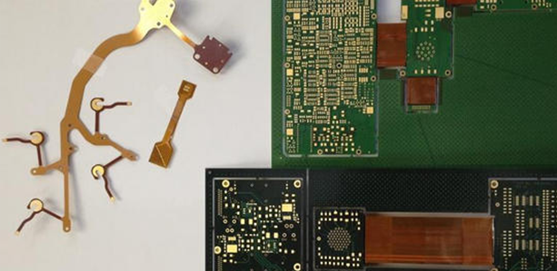
Key Rigid-Flex Manufacturing Steps
Flex Circuit Fabrication
- Polyimide base film: 12.5μm, 25μm, 50μm thickness per IPC‑4203
- Copper foil: 12μm rolled annealed (RA) for dynamic flex, 18μm electrodeposited (ED) for static use
- Coverlay application: 25μm adhesive-coated PI, laminated at 160–180°C
- Minimum line width/space: 50μm/50μm for flex regions, ±8μm tolerance
- Bend radius control: static ≥6× board thickness, dynamic ≥15× board thickness
Learn more about: Flexible PCB: A Comprehensive Guide to Features, Applications, Types & Key Considerations
Rigid Preparation
- FR‑4 core: 0.2mm–1.0mm thickness, Tg 140–170°C
- Prepreg: 1080, 2116 styles with low-flow adhesive for rigid‑flex bonding
- Inner layer imaging: LDI exposure with ±10μm registration
- Etching control: uniform etch factor ≥2.5, undercut ≤15μm
- AOI inspection: 100% coverage for opens, shorts, and line width variation
Bonding and Integration
- Rigid‑flex stack-up lamination: 170–190°C, 20–25 kg/cm², 60–90 minute cycle
- Adhesive selection: modified acrylic or epoxy with <1% void rate post‑lamination
- Step‑milling for flex access: controlled depth to 0.1mm tolerance
- Stress relief at rigid‑flex transition: 0.5mm clearance zone, no vias or components
Step-by-Step Rigid-Flex PCB Manufacturing
Material Preparation & Inner Layer Processing
- Cut PI flex films and FR‑4 rigid cores to panel size (406×508mm standard)
- Clean surfaces via plasma treatment to improve adhesion
- Apply dry film photoresist: 15–20μm thickness for flex, 25–30μm for rigid
- Expose and develop inner layer circuits per IPC‑2221
- Etch copper and strip resist; AOI scan to eliminate defects
- Black oxide treatment on rigid inner layers for bonding strength
Drilling, Plating & Metallization
- Mechanical drilling: 0.2mm minimum hole size, aspect ratio ≤8:1
- Laser drilling: 100μm microvias in flex regions, depth control ±10μm
- Desmear: plasma etch for flex, permanganate for rigid to remove resin smear
- Electroless copper deposition: 0.3–0.5μm base layer
- Electroplating: 20–25μm total copper thickness in holes, uniform distribution
- Panel plating: line width compensation to maintain target tolerance
Lamination, Coverlay & Final Processing
- Lay up prepreg, flex cores, and rigid frames in symmetrical stack-up
- Vacuum lamination with controlled ramp rate to prevent voiding
- Laser profile routing for flex bend areas and outer contours
- Solder mask: liquid photoimageable (LPI), 15–20μm thickness
- Surface finish: ENIG (2–5μm Ni, 0.05–0.1μm Au), immersion tin, or hard gold
- Final cleaning and baking at 120°C for 60 minutes to remove moisture
Testing and Verification
Electrical Testing
- Flying probe test: 100% net continuity, isolation resistance ≥100MΩ
- Impedance measurement: ±10% tolerance per IPC‑2221
- Microsection analysis: via barrel integrity, copper distribution, lamination quality
- Resistance check: via resistance ≤5mΩ for reliable interconnection
Reliability Validation
- Thermal cycling: -40°C to +125°C, 100 cycles, no delamination
- Flex fatigue test: dynamic bending 1,000–10,000 cycles without open circuits
- Solder resistance: 260°C, 10 seconds, 3x reflow with no blistering
- Peel strength: rigid‑flex bond ≥1.0 N/mm per IPC‑6012 Class 3
Capabilities and Advantages
Layer Count & Design Flexibility
- Layer range: 2–16 total layers, 1–4 flex layers
- Dynamic flex zones: repeated bending up to 100,000 cycles
- 3D form factor: fits irregular enclosures, eliminates connectors
- Stack-up symmetry: minimizes warpage to ≤0.5% across panel
Reliability & Material Performance
- Materials: PI, FR‑4, high‑Tg resins, low‑CTE adhesives
- Operating temperature: -55°C to +150°C
- Moisture sensitivity: MSL 3 compliant after proper baking
- Vibration resistance: meets MIL‑STD‑202 requirements
Critical Considerations
Layer Structure & Adhesive Use
- Symmetrical layer balance to avoid warping
- Adhesive thickness: 12–25μm for flex bonding, no bleed‑out
- No adhesive coverage over dynamic bend lines
- Transition zone design: gradual taper to reduce stress concentration
Precision & Cost Drivers
- Registration tolerance: ±20μm layer‑to‑layer
- Minimum features: 50μm lines, 100μm laser vias
- Cost increases with layer count, flex length, and microvia density
- Prototype lead time: 7–10 days; mass production: 14–21 days
Comparative Tables
Rigid-Flex vs. Rigid PCB Only
| Parameter | Rigid-Flex PCB | Rigid PCB Only | Benefit |
|---|---|---|---|
| Assembly Density | 40% higher | Standard | Space savings |
| Interconnection Reliability | 3x higher | Base | Fewer connectors |
| Bend Capability | Dynamic/static | None | 3D routing |
| Warpage Control | ≤0.5% | ≤0.7% | Better assembly |
| Cost | +25–40% | Base | Performance offset |
Flex Materials: RA Copper vs. ED Copper
| Parameter | Rolled Annealed (RA) | Electrodeposited (ED) | Best Use |
|---|---|---|---|
| Flex Life | 10,000+ cycles | 1,000 cycles | Dynamic bending |
| Ductility | High | Moderate | Repeated motion |
| Cost | +15% | Standard | Static flex |
| Thickness | 12μm standard | 18μm standard | Fine lines |
Core Technical Parameters
- Minimum line width/space: 50μm/50μm (flex), 40μm/40μm (rigid)
- Minimum hole size: 0.2mm mechanical, 100μm laser
- Aspect ratio: ≤8:1 (mechanical), ≤1:1 (laser)
- Board thickness: 0.4mm–2.0mm
- Impedance tolerance: ±10% (IPC‑2221)
- Registration accuracy: ±20μm
- Bend radius: static ≥6× t, dynamic ≥15× t
- Surface finishes: ENIG, HASL, immersion tin, hard gold
Case Study
Project Overview
8‑layer rigid flex circuit boards for wearable medical device: 2 flex layers, 6 rigid layers, 0.8mm total thickness, 100μm laser vias, 50μm/50μm line/space, ENIG finish, IPC‑6012 Class 2.
Initial Challenges
- Delamination at rigid‑flex transition after 50 thermal cycles
- Flex zone copper cracking after 800 bending cycles
- Via voiding in plated through‑holes
- Warpage of 0.8% exceeding 0.5% limit
- First‑pass yield at 76%
Process Improvements
- Implemented symmetrical stack-up with balanced copper distribution
- Changed ED copper to 12μm RA copper in flex regions
- Optimized lamination temperature ramp and vacuum hold time
- Added stress relief slots at rigid‑flex boundaries
- Enhanced desmear and pulse plating for via filling
- Introduced post‑lamination baking to reduce moisture
Final Results
- Delamination eliminated across 100 thermal cycles
- Flex life extended to 12,000 cycles without failure
- Via void rate reduced to <1%
- Warpage controlled to 0.35%
- First‑pass yield improved to 90.5%
- Zero field failures reported in customer validation
Common Design Errors
Feature & Layout Violations
- Specifying bend radius <6× board thickness causing copper fracture
- Placing vias or components within 0.5mm of rigid‑flex transition
- Designing line width <40μm beyond standard fabrication capability
- Asymmetrical stack-up leading to warpage >0.5%
- Inadequate annular ring: <75μm for 0.2mm holes
Material & Process Misalignment
- Using standard Tg <140°C materials for high‑temp applications
- Excessive adhesive thickness causing bleed and contamination
- Missing coverlay in flex zones leading to short circuits
- Ignoring manufacturer DFM rules for via size and spacing
- Inconsistent copper weight creating etching variation
Assembly & Testing Conflicts
- Insufficient test points for full electrical coverage
- Component placement too close to flex bend areas
- Improper solder mask expansion causing solder bridging
- Lack of stress relief in high‑flex regions
- Ignoring impedance requirements for high‑speed signals
Frequently Asked Questions
Q1: What is the minimum bend radius for rigid-flex PCB?
A1: Static bending requires a minimum radius of 6× the board thickness; dynamic bending needs 15× thickness to prevent copper fatigue and fracture.
Q2: What materials are used in rigid-flex PCB manufacturing?
A2: Flexible regions use polyimide (PI) film with rolled or electrodeposited copper; rigid sections use FR‑4 cores with high‑Tg prepreg and low‑flow adhesives for bonding.
Q3: How does rigid-flex PCB differ from flexible printed circuit alone?
A3: Rigid-flex PCB combines structural rigid areas for component mounting with flexible zones for 3D routing, while flexible PCB lacks structural support and requires additional stiffeners.
Q4: What IPC standards govern rigid-flex PCB manufacturing?
A4: Rigid-flex fabrication follows IPC‑6012 for specification, IPC‑2221 for design rules, IPC‑4203 for flex materials, and IPC‑9701 for reliability testing.
If you need professional rigid flex PCB design support or quotation, our team provides free DFM check and fast turnaround.


![Understanding PCB Costs & Pricing [Your Complete Guide]](https://hdicircuitboard.com/wp-content/uploads/elementor/thumbs/Understanding-PCB-Costs-Pricing-Your-Complete-Guide-qzzhe6mcaxuolkux3xalfktgavumi9y1aqfbs9bpv4.webp "Understanding PCB Costs & Pricing [Your Complete Guide]")


