
Signal Integrity in HDI PCB Design: Expert Strategies for Reliable High-Density Interconnect Performance
High Density Interconnect (HDI) PCBs are the backbone of modern electronics, powering devices from smartphones to aerospace systems with their compact layouts, microvias, and dense component placement. Signal Integrity (SI) in HDI PCB design ensures electrical signals propagate without distortion, crosstalk, or loss—critical for maintaining functionality in high-speed, high-frequency applications. This comprehensive guide breaks down core SI concepts, actionable design tips, and solutions to common challenges, tailored specifically for HDI PCBs, including flexible pcb, rigid flex pcb, and rf pcb implementations.
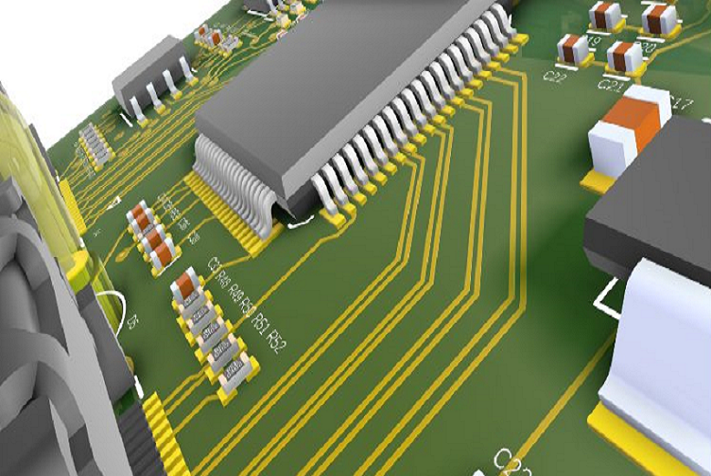
Learn more about: High Speed HDI PCB Design Guide
What is Signal Integrity in PCB?
Signal Integrity (SI) refers to a signal’s ability to travel from source to receiver without degradation, preserving its original quality and timing. In PCBs, SI encompasses the minimization of unwanted effects like reflections, crosstalk, electromagnetic interference (EMI), and signal attenuation. For HDI PCBs—characterized by fine traces, microvias, and high component density—SI is even more critical due to tighter spacing and increased susceptibility to parasitic effects.
Key Principles of Signal Integrity
- Signal Quality: Signals must retain their waveform shape, avoiding overshoot, undershoot, or ringing that can cause data errors.
- Timing Accuracy: Signals must arrive at their destination within specified time windows to meet setup and hold requirements, especially in synchronous systems.
- Noise Immunity: Signals must resist interference from adjacent traces, power planes, or external sources (EMI).
- Consistent Impedance: Maintaining controlled impedance throughout transmission lines prevents reflections that distort signals.
Why SI Matters for HDI PCBs
HDI PCBs push the limits of miniaturization, with trace widths as small as 25 microns (1 mil), microvias under 6 mils, and component pitches down to 0.4mm. These tight tolerances increase the risk of SI issues:
- Fine traces are more prone to signal attenuation and crosstalk.
- Microvias and blind vias introduce impedance discontinuities if not designed properly.
- Dense component placement reduces spacing between signal paths, amplifying interference.
- High-speed interfaces (e.g., PCIe, DDR5, Ethernet) in HDI circuit boards demand precise SI to support data rates exceeding 10 Gbps.
Key Aspects of HDI Signal Integrity
Microvias and Via-in-Pad
Microvias (diameter ≤6 mils) and via-in-pad technology are defining features of HDI PCBs, enabling high routing density but requiring careful SI consideration:
- Microvia Design: Laser-drilled microvias minimize stub length, a major source of reflections in high-speed designs. For optimal SI, microvias should have an aspect ratio ≤0.75:1 (drill depth to diameter) to ensure reliable plating and reduce parasitic capacitance.
- Via-in-Pad (VIPPO): Placing microvias directly within component pads shortens signal paths, reducing inductance and improving SI. VIPPO requires non-conductive epoxy filling and plating to maintain planarity, critical for fine-pitch BGAs and SMT components.
- Stacked vs. Staggered Vias: Stacked vias offer maximum density but require precise alignment to avoid impedance jumps. Staggered vias reduce manufacturing complexity and improve SI by minimizing voids and planarization needs.
Layer Stackup & Reference Planes
Layer stackup design is foundational to HDI SI, as it dictates impedance control, return path continuity, and crosstalk mitigation:
- Symmetrical Stackups: Symmetrical layer configurations (e.g., signal-ground-signal-power-ground-signal) reduce board warpage and ensure consistent electrical performance across all layers.
- Reference Plane Continuity: High-speed signal layers must be adjacent to solid ground or power planes to provide low-impedance return paths. Discontinuities (splits, slots, or voids) force return currents to detour, increasing loop inductance and degrading SI.
- Layer Pairing: For differential signals, route pairs on the same layer between two reference planes (stripline configuration) to maintain symmetry and minimize crosstalk. For single-ended signals, use microstrip (outer layer with adjacent ground plane) for cost-effectiveness.
- HDI-Specific Stackups: Sequential lamination in HDI PCBs allows for blind/buried vias and microvia integration, but limits lamination cycles to 3 for SI stability.
Impedance Control
Controlled impedance is non-negotiable for SI in HDI PCBs, as impedance mismatches cause signal reflections and timing errors:
- Target Impedance Values: Industry standards specify typical values: 50Ω for single-ended signals, 90Ω–100Ω for differential pairs (e.g., PCIe, USB 3.0), and 75Ω for RF signals in rf pcb designs.
- Impedance Calculation Factors: Impedance depends on trace width, spacing, dielectric thickness, and dielectric constant (Dk). Tools like Polar SI9000 or CAD-integrated calculators (Altium, Cadence) help optimize these parameters.
- Manufacturing Tolerances: HDI PCBs require tight impedance tolerances (±5% for critical signals), achievable through precise control of dielectric thickness (±10%) and trace width (±3%).
- Impedance Verification: Use TDR (Time Domain Reflectometry) coupons during production to validate impedance compliance with IPC-6012 Class 3 standards.
Trace Routing
Trace routing directly impacts SI in HDI PCBs, with fine-pitch components and dense layouts demanding precision:
- Trace Width & Spacing: For HDI designs, trace widths range from 1–3 mils (25–75 microns) for signal lines, with spacing equal to or greater than trace width to minimize crosstalk. Follow the 3W rule (spacing = 3× trace width) for critical signals.
- Differential Pair Routing: Route differential pairs in parallel with consistent spacing to maintain impedance symmetry. Keep lengths matched within 20 mils to avoid skew, and avoid vias or component placements between pairs.
- Trace Bends: Use 45° bends or rounded corners instead of 90° bends to reduce impedance discontinuities. Serpentine traces for length matching should have minimum segment lengths (1.5× trace width) and spacing (4× trace width) to avoid SI degradation.
- Layer Transitions: Minimize layer changes for high-speed signals. When necessary, use stitching vias (ground vias adjacent to signal vias) to maintain return path continuity.
Crosstalk Mitigation
Crosstalk—unwanted coupling between adjacent traces—is a top SI concern in HDI PCBs due to tight spacing:
- Spacing Optimization: Increase spacing between high-speed traces and noisy signals (e.g., clock lines) to reduce capacitive and inductive coupling. For differential pairs, maintain consistent spacing to reject common-mode noise.
- Ground Plane Shielding: Place ground planes between signal layers to isolate traces. For critical signals, use guard traces (grounded traces) between signal paths to absorb coupled noise.
- Orthogonal Routing: Route traces on adjacent layers at 90° to each other to minimize crosstalk, as magnetic fields between orthogonal traces do not couple.
- Length Limitation: Limit parallel trace runs to less than 1/10 of the signal wavelength to reduce crosstalk. For a 10 GHz signal, this translates to ~0.5 inches (12.7mm) of parallel routing.
Material Selection
PCB materials directly influence SI in HDI designs, affecting signal loss, impedance stability, and crosstalk:
- Dielectric Constant (Dk): Low-Dk materials (Dk = 3.0–3.8) reduce signal propagation delay and crosstalk. Examples include Rogers RO4350, Isola I-Speed, and Megtron 8, ideal for rf pcb and high-speed HDI applications.
- Dissipation Factor (Df): Low-Df materials (Df < 0.005) minimize dielectric loss, critical for high-frequency signals (≥5 GHz). PTFE-based materials (e.g., Rogers RO3003) offer ultra-low Df for demanding RF applications.
- Copper Foil: Smoother copper foils (e.g., reverse-treated foil) reduce skin effect loss at high frequencies, improving SI in fine-trace HDI designs.
- Thermal Stability: Materials with high glass transition temperature (Tg ≥180°C) prevent dielectric degradation under thermal stress, maintaining Dk stability and SI over the product lifecycle.
Decoupling
Power Integrity (PI) directly impacts SI, as PDN (Power Distribution Network) noise couples into signal paths. Effective decoupling is essential for HDI PCBs:
- Decoupling Capacitor Placement: Place ceramic decoupling capacitors (0.1µF, 1µF, 10µF) within 50 mils of IC power pins to minimize loop inductance. Use multiple capacitor values to cover a wide frequency spectrum (100 kHz–1 GHz).
- Capacitor Selection: Choose low-ESR (Equivalent Series Resistance) and low-ESL (Equivalent Series Inductance) capacitors to maximize decoupling effectiveness at high frequencies.
- Power Plane Design: Use solid power and ground planes to reduce PDN impedance. Place power planes adjacent to ground planes to increase interplane capacitance, further stabilizing voltage.
- Stitching Capacitors: Use stitching capacitors (10nF–100nF) between split planes or different ground domains to provide low-impedance paths for return currents, preventing SI degradation.
HDI Design Tips for Signal Integrity
Avoid Via Stubs
Via stubs (unused portions of through-holes or blind vias) act as resonant circuits, causing reflections and signal loss at high frequencies:
- Backdrilling: Remove via stubs using backdrilling for through-holes in high-speed HDI designs, reducing stub length to less than 10 mils.
- Blind/Buried Vias: Use blind vias (connect outer to inner layers) and buried vias (connect inner layers) to eliminate stubs entirely, ideal for multilayer pcb and HDI rigid flex pcb designs.
- Microvia Implementation: Laser-drilled microvias (≤6 mils) naturally have short stubs, making them optimal for high-speed signals in HDI circuit boards.
Symmetry
Symmetrical design minimizes impedance mismatches and crosstalk in HDI PCBs:
- Differential Pair Symmetry: Route differential pairs with identical lengths, spacing, and bend geometries to maintain impedance balance and common-mode noise rejection.
- Layer Symmetry: Design symmetrical stackups to ensure consistent signal propagation speeds across all layers, reducing timing skew.
- Component Placement: Symmetrically place components around critical signal paths to balance parasitic effects and reduce EMI.
Return Path Continuity
Uninterrupted return paths are critical for SI, as broken paths increase loop inductance and noise:
- Solid Reference Planes: Avoid splits or slots in ground/power planes under high-speed traces. If splits are necessary, route signals around them or use stitching capacitors to bridge the gap.
- Via Placement: Place ground vias adjacent to signal vias (within 20 mils) when changing layers, providing a continuous return path and reducing loop inductance.
- Avoid Trace Over Splits: Never route high-speed signals over split planes, as this forces return currents to take longer paths, degrading SI.
Common Signal Integrity Challenges in HDI
Impedance Mismatch
Impedance mismatch occurs when trace geometry, dielectric properties, or via design deviates from target values, causing signal reflections:
- Causes: Inconsistent trace width, dielectric thickness variations, via diameter changes, or poor layer registration.
- Effects: Ringing, overshoot, undershoot, and timing errors, leading to data corruption in high-speed interfaces.
- Solutions:
- Use CAD tools to enforce consistent trace width and spacing.
- Verify dielectric thickness with manufacturer data sheets and TDR testing.
- Design vias with consistent pad sizes and annular rings (minimum 2 mils for outer layers per IPC-2221).
- Implement series termination resistors (50Ω–100Ω) at signal sources to match impedance.
Crosstalk
Crosstalk is the transfer of energy between adjacent traces, caused by capacitive (electric field) and inductive (magnetic field) coupling:
- Causes: Tight trace spacing, long parallel runs, lack of ground plane shielding, and high signal rise/fall times.
- Effects: Signal distortion, false triggers, and reduced noise margins, particularly problematic in dense HDI layouts.
- Solutions:
- Increase trace spacing to at least 3× trace width (3W rule) for critical signals.
- Use ground planes or guard traces to isolate sensitive signals (e.g., RF paths in rf pcb designs).
- Limit parallel trace runs to less than 1/10 the signal wavelength.
- Route differential pairs tightly coupled (spacing = 0.5×–1× trace width) to reject crosstalk.
Signal Loss/Attenuation
Signal loss occurs as signals propagate through traces and vias, caused by conductor resistance, dielectric loss, and skin effect:
- Causes: Fine trace widths (increased resistance), high-Df materials (dielectric loss), copper roughness (skin effect), and via resistance.
- Effects: Reduced signal amplitude, increased rise time, and data errors in long or high-frequency paths.
- Solutions:
- Use wider traces (≥3 mils) for critical signals to reduce resistance.
- Select low-Df materials (e.g., Rogers RO4350, Isola Tachyon 100G) to minimize dielectric loss.
- Choose smooth copper foils to reduce skin effect loss at high frequencies.
- Minimize via count and use plated-through holes with sufficient copper thickness (≥20µm) to reduce via resistance.
EMI/EMC Issues
HDI PCBs are prone to EMI due to dense traces and high-speed signals, which can cause SI degradation and non-compliance with regulatory standards:
- Causes: Unshielded signal paths, large current loops, and poor grounding.
- Effects: Signal interference, reduced SI, and failure to meet FCC or CE EMC requirements.
- Solutions:
- Use ground planes as shields between signal layers.
- Minimize current loop areas by placing power and ground planes close together.
- Route high-speed signals away from board edges and connectors (major EMI radiators).
- Implement EMI shielding for critical sections (e.g., RF modules in rf pcb designs) using conductive enclosures or shielding layers.
Critical Considerations for Specialized HDI PCBs
HDI Flexible PCB & HDI Rigid Flex PCB
Flexible and rigid flex HDI PCBs introduce unique SI challenges due to their flexible substrates and dynamic use cases:
- Material Selection: Use flexible dielectrics (e.g., polyimide) with stable Dk (3.0–3.5) and low Df to maintain SI during bending.
- Trace Routing: Avoid sharp bends (minimum bend radius = 10× board thickness) to prevent trace damage and impedance changes.
- Via Design: Use microvias and blind vias to minimize substrate thickness and improve flexibility without compromising SI.
- Grounding: Implement continuous ground planes across flexible and rigid sections to maintain return path continuity.
RF PCB & High-Frequency HDI
RF PCBs and high-frequency HDI designs (≥5 GHz) demand strict SI control to minimize signal loss and interference:
- Impedance Precision: Maintain impedance tolerance ±3% for RF signals, using low-Dk/low-Df materials (e.g., PTFE, Rogers RO3003).
- Trace Geometry: Use controlled-impedance microstrips or striplines with consistent width and spacing to avoid signal reflections.
- Shielding: Implement coplanar waveguides or shielding layers to isolate RF paths from other signals.
- Component Integration: Place RF components (e.g., antennas, filters) close to signal paths to minimize trace length and loss.
FAQ: Signal Integrity in HDI PCB Design
What is the Difference Between SI and PI in HDI PCBs?
Signal Integrity (SI) focuses on signal quality and propagation, while Power Integrity (PI) ensures stable power delivery. PI directly impacts SI—PDN noise couples into signal paths, causing distortion. In HDI PCBs, PI is critical due to dense power distribution, making decoupling and solid power planes essential for both PI and SI.
How Does Trace Width Affect SI in HDI PCBs?
Trace width influences resistance, capacitance, and impedance. Narrow traces (≤2 mils) increase resistance and signal loss, while overly wide traces increase capacitance, causing slower rise times. For HDI designs, trace widths of 2–4 mils balance SI, manufacturability, and density.
What IPC Standards Govern SI in HDI PCBs?
Key IPC standards include:
- IPC-2221: Provides general guidelines for trace spacing, impedance control, and component placement.
- IPC-6012: Specifies performance requirements for rigid PCBs, including impedance tolerance and via quality.
- IPC-2226: Details HDI-specific design rules, including microvia dimensions and sequential lamination.
- IPC-TM-650: Outlines test methods for SI verification (e.g., TDR, crosstalk measurements).
How to Choose Between Stacked and Staggered Vias for SI?
Stacked vias offer maximum density but require precise alignment to avoid impedance jumps. They are ideal for space-constrained HDI circuit boards but may increase manufacturing complexity. Staggered vias reduce voids and planarization needs, improving SI and manufacturability, making them preferable for high-speed designs where density is less critical.
H3: Can HDI PCBs Achieve SI Performance Comparable to Standard PCBs?
Yes—with proper design, HDI PCBs can match or exceed standard PCB SI performance. By using microvias, controlled-impedance routing, and low-loss materials, HDI designs minimize parasitic effects, making them suitable for high-speed applications like 5G, DDR5, and PCIe 5.0.
Conclusion
Signal Integrity in HDI PCB design is a multifaceted discipline that requires careful attention to layer stackup, trace routing, via technology, material selection, and decoupling. By implementing the strategies outlined in this guide—such as controlled impedance, continuous return paths, crosstalk mitigation, and microvia optimization—designers can overcome the unique challenges of HDI PCBs, including flexible pcb, rigid flex pcb, and rf pcb implementations. Adhering to IPC standards and leveraging advanced CAD tools and simulation software ensures that HDI circuit boards deliver reliable, high-performance SI for even the most demanding applications. As electronics continue to miniaturize and speed up, mastering SI in HDI design remains a critical skill for engineers aiming to create innovative, reliable products.


![Understanding PCB Costs & Pricing [Your Complete Guide]](https://hdicircuitboard.com/wp-content/uploads/elementor/thumbs/Understanding-PCB-Costs-Pricing-Your-Complete-Guide-qzzhe6mcaxuolkux3xalfktgavumi9y1aqfbs9bpv4.webp "Understanding PCB Costs & Pricing [Your Complete Guide]")


