
Ultra HDI PCB Manufacturing Capabilities & Design: Master High-Density Interconnect for Next-Gen Electronics
Ultra High-Density Interconnect (UHDI) PCB technology redefines the boundaries of miniaturization and performance for electronic devices. As demand grows for smaller, faster, and more reliable electronics—from 5G mmWave modules to medical implants—UHDI emerges as the solution to overcome the limitations of standard HDI. This comprehensive guide details UHDI manufacturing capabilities, design essentials, and critical considerations for integrating UHDI into rigid flex pcb, flexible pcb, flexible printed circuit, rf pcb, and multilayer pcb applications, grounded in IPC standards and two decades of industry expertise.
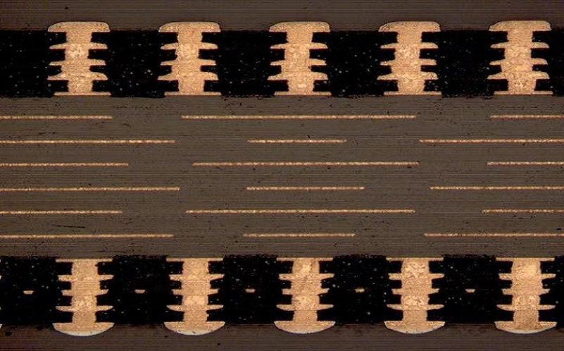
Learn more about: How to Design HDI Microvia PCB
Foundational Definitions: What Are Standard HDI and UHDI PCBs?
What Is Standard HDI PCB?
Standard HDI (High-Density Interconnect) PCB is defined by IPC-2226 as a printed circuit board utilizing microvias (≤0.15mm finished diameter), fine trace/space (down to 0.1mm/0.1mm), and sequential lamination to achieve higher component density than traditional PCBs. Key characteristics include microvia diameters ranging from 0.08mm to 0.15mm with aspect ratios up to 1:1, trace width and spacing between 0.075mm (3mil) and 0.1mm (4mil), and support for blind vias, buried vias, and via-in-pad configurations. It is compatible with fine-pitch components (0.5mm–0.8mm pitch BGAs) and typically features layer counts between 4 and 30+ with dielectric thickness ≤0.127mm (5mil), making it ideal for smartphones, tablets, IoT devices, and automotive sensor modules.
What Is UHDI High Density Interconnect PCB?
UHDI (Ultra High-Density Interconnect) PCB represents the next evolution of HDI technology, characterized by ultra-fine features, tighter tolerances, and extreme routing density. Defined by trace/space ≤0.05mm (2mil) and microvia diameters <0.075mm (3mil), UHDI enables unprecedented component packing and signal performance. Core attributes include trace width and spacing as low as 0.025mm (1mil) for advanced applications, microvia diameters down to 0.025mm (1mil) with copper-filled construction, and dielectric thickness ≤0.03mm (1.2mil) to minimize signal loss and board thickness. It supports stacked/staggered microvias and any-layer interconnects, works with ultra-fine-pitch components (≤0.4mm pitch BGAs), and can achieve board thickness as thin as 0.4mm (16mil) for compact devices like wearables and medical implants.
UHDI vs Standard HDI PCB: Key Differences
The distinction between UHDI and standard HDI lies in feature size, tolerances, and manufacturing complexity—directly impacting performance, cost, and application suitability. Below is a detailed comparison that addresses common decision-making challenges:
| Parameter | Standard HDI PCB | UHDI PCB |
|---|---|---|
| Trace Width/Spacing | 0.075mm–0.1mm (3–4mil) | ≤0.05mm (2mil), down to 0.025mm (1mil) |
| Microvia Diameter | 0.08mm–0.15mm (3.2–6mil) | <0.075mm (3mil), down to 0.025mm (1mil) |
| Dielectric Thickness | ≤0.127mm (5mil) | ≤0.03mm (1.2mil) |
| Component Pitch Compatibility | 0.5mm–0.8mm | ≤0.4mm |
| Layer Count Range | 4–30+ | 6–12+ (fewer layers for same density) |
| Via Types | Blind, buried, microvia, via-in-pad | Stacked/staggered microvias, via-in-pad (VIPPO) |
| Impedance Tolerance | ±7% | ±5% |
| Board Thickness | <1mm (40mil) | ≤0.4mm (16mil) |
| Component Density | High | Very high (up to 2x standard HDI) |
| Manufacturing Process | Sequential lamination, LDI imaging | SAP/mSAP, embedded trace technology, laser drilling |
| Typical Applications | Smartphones, tablets, IoT devices | Wearables, medical implants, 5G mmWave, AI systems |
Practical implications of these differences are critical for design decisions: UHDI’s thinner dielectrics and shorter trace lengths reduce parasitic capacitance/inductance, enabling data rates up to 100Gbps—essential for rf pcb and high-speed digital applications. For miniaturization-focused projects like flexible printed circuit and HDI rigid flex pcb in wearables, UHDI reduces PCB footprint by 30–50% compared to standard HDI. However, UHDI’s tighter tolerances and specialized processes increase manufacturing costs by 20–40%, justifying adoption only for high-value, space-constrained applications where performance cannot be compromised.
Key Design Considerations for UHDI
Trace/Space Goals
UHDI trace and space dimensions directly impact routing density, signal integrity, and manufacturability, with industry-proven targets tailored to resolve common design challenges. Standard UHDI applications use 0.05mm (2mil) trace / 0.05mm (2mil) space for general areas, while advanced designs leverage 0.03mm (1.2mil) trace / 0.03mm (1.2mil) space for high-density regions. Critical RF paths require 0.04mm (1.6mil) trace / 0.06mm (2.4mil) space to minimize crosstalk, a key concern for rf pcb performance. Power traces demand a minimum 0.1mm (4mil) width for 1A current (adjustable based on copper thickness) to prevent overheating. Tolerance control is paramount: trace width tolerance shrinks from ±10% (standard HDI) to ±5% (UHDI) for features ≤0.05mm, requiring advanced etching processes like mSAP to maintain precision.
Via Technology
Vias are the backbone of UHDI interconnects, with design choices directly affecting density, signal integrity, and reliability. Copper-filled microvias (VIPPO) are recommended for structural stability and thermal conductivity, with diameters matching dielectric thickness to maintain a 1:1 aspect ratio—critical for preventing voids during fabrication. Stacked microvias maximize density by routing through multiple layers vertically, while staggered microvias reduce dielectric stress and improve signal integrity for high-speed paths. For via-in-pad designs, solder mask defined (SMD) pads are preferred over non-solder mask defined (NSMD) to avoid solder bridging in ultra-fine-pitch BGA applications. Blind vias should be limited to 2–3 layers deep to ensure plating uniformity, a common pain point in UHDI manufacturing that impacts long-term reliability.
Material Selection
Material choice is a make-or-break factor for UHDI performance, as standard FR-4 often fails to meet thermal, mechanical, or signal integrity requirements. For high-speed digital and rf pcb applications, low-loss dielectrics like Rogers 4350B (Dk=3.48, Df=0.0037) or Isola FR408HR (Dk=3.66, Df=0.008) minimize signal attenuation at frequencies above 10GHz. Flexible printed circuit and HDI rigid flex pcb require polyimide (PI) substrates with low coefficient of thermal expansion (CTE) to withstand repeated bending and thermal cycling. Copper thickness plays a critical role: 12μm (0.5oz) copper is standard for UHDI to support fine trace etching, while 18μm (1oz) copper is used for power layers to handle higher currents. For medical and aerospace applications, halogen-free materials meeting IPC-4101/21 requirements ensure compliance with environmental and safety standards.
Design Rules
Adhering to strict design rules is essential to avoid manufacturability issues and ensure UHDI performance. Key rules include:
- Trace width consistency: Avoid abrupt width changes to prevent signal reflections; use tapered transitions (1:3 ratio) when adjustments are necessary.
- Minimum annular ring: Maintain ≥0.02mm (0.8mil) annular ring for microvias to ensure plating coverage, per IPC-6012 Class 3 requirements.
- Clearance between vias and components: Keep ≥0.1mm (4mil) clearance between microvias and BGA pads to prevent solder wicking.
- Thermal relief for power pads: Implement 4-point thermal relief for power pads to balance heat dissipation and solderability.
- Routing for RF paths: Use curved traces (minimum radius = 3x trace width) for rf pcb to minimize signal loss and impedance variation.
- Ground plane design: Provide continuous ground planes for high-speed signals, with ≤0.5mm distance between signal layers and ground planes to control impedance.
Layer Stackup for UHDI
Layer stackup design directly impacts UHDI performance, with careful consideration of signal routing, power distribution, and thermal management. For rigid flex pcb and HDI rigid flex pcb, stackup must balance rigidity (for component mounting) and flexibility (for dynamic applications). Key guidelines include:
- Symmetrical stackup: Use symmetrical layer configurations (e.g., signal-dielectric-ground-ground-dielectric-signal) to minimize board warpage during lamination, a critical issue for UHDI due to thinner dielectrics.
- Dielectric thickness control: Maintain consistent dielectric thickness (±0.005mm) between signal layers to ensure uniform impedance—critical for high-speed and rf pcb applications.
- Power layer placement: Position power layers adjacent to ground planes to reduce electromagnetic interference (EMI) and improve power delivery.
- Layer count optimization: UHDI enables 30% fewer layers than standard HDI for the same density; for example, a 12-layer UHDI board can replace an 18-layer standard HDI board.
- Flexible section design: For flexible printed circuit, use 2–4 signal layers with polyimide dielectric (0.025mm–0.05mm thick) and coverlay (0.02mm thick) to protect traces during bending.
Example stackup for a 6-layer UHDI rigid flex pcb:
- Top rigid layer: 12μm copper (signal) + 0.03mm low-loss dielectric
- Rigid ground layer: 18μm copper + 0.03mm low-loss dielectric
- Flexible signal layer: 12μm copper + 0.025mm polyimide dielectric
- Flexible signal layer: 12μm copper + 0.025mm polyimide dielectric
- Rigid ground layer: 18μm copper + 0.03mm low-loss dielectric
- Bottom rigid layer: 12μm copper (signal)
Fabrication Processes and Techniques for UHDI
SAP/mSAP Technology
Semi-Additive Process (SAP) and Modified Semi-Additive Process (mSAP) are the foundation of UHDI fabrication, enabling ultra-fine trace widths down to 0.025mm (1mil). SAP involves:
- Laminating a thin copper foil (1μm–3μm) to the dielectric substrate.
- Applying and patterning photoresist to define trace areas.
- Electroplating copper (to desired thickness: 10μm–15μm) on exposed areas.
- Stripping photoresist and etching the thin base copper to remove unwanted areas.
mSAP enhances SAP by adding a tin plating step before resist stripping, which acts as an etch mask—improving trace edge definition and reducing sidewall roughness to <2μm. This process is mandatory for UHDI traces ≤0.05mm (2mil), as traditional subtractive etching cannot achieve the required precision.
Laser Drilling
Laser drilling is critical for creating UHDI microvias, with UV lasers (355nm wavelength) being the industry standard for their precision. Key parameters include:
- Drill diameter: Down to 0.025mm (1mil) with ±0.002mm tolerance.
- Aspect ratio: Limited to 1:1 for blind vias to ensure uniform plating.
- Drill speed: Up to 100,000 holes per minute for high-volume production.
- Deburring: Plasma deburring is used to remove dielectric residue (smear) from hole walls, preventing signal degradation and plating defects.
For stacked microvias, laser drilling is performed sequentially after each lamination step, with alignment accuracy of ±0.005mm to ensure via registration—critical for avoiding interlayer shorts.
Imaging
UHDI imaging relies on Laser Direct Imaging (LDI) technology, which replaces traditional photomasks with high-precision lasers to pattern photoresist. LDI offers:
- Resolution: Down to 0.01mm (0.4mil) for ultra-fine features.
- Alignment accuracy: ±0.002mm between layers, essential for UHDI’s tight pitch requirements.
- Flexibility: Enables rapid design changes without costly photomask revisions.
- Uniformity: Consistent exposure across the board to ensure trace width uniformity.
For rf pcb and high-speed designs, LDI is paired with high-resolution photoresists (≥0.5μm resolution) to maintain critical dimensions for impedance control.
Etching
Etching for UHDI requires precise control to avoid over-etching or under-etching ultra-fine traces. Key techniques include:
- Acid copper etching: Use of cupric chloride-based etchants with controlled temperature (30°C–40°C) and spray pressure (0.2MPa–0.3MPa).
- Etch factor optimization: Maintain an etch factor of ≥4:1 to minimize trace sidewall taper, ensuring trace width accuracy.
- In-situ etch monitoring: Real-time monitoring of etch progress using optical sensors to stop etching at the exact moment required.
- Post-etch cleaning: Thorough cleaning to remove etchant residues, which can cause corrosion and reliability issues.
Best Practices for UHDI Design and Manufacturing
Early Engagement
Collaboration between designers and manufacturers early in the design cycle reduces iterations and ensures manufacturability. Key steps include:
- Sharing preliminary designs with manufacturers to identify potential issues (e.g., tight clearances, incompatible materials).
- Reviewing manufacturing capabilities (e.g., minimum trace/space, microvia diameter) to align design with process limits.
- Conducting Design for Manufacturability (DFM) reviews before finalizing Gerber files, focusing on trace geometry, via placement, and layer stackup.
Simulation
Simulation is critical for UHDI to predict and resolve performance issues before fabrication. Key simulation types include:
- Signal integrity (SI) simulation: Use tools like Ansys HFSS or Cadence Allegro to analyze crosstalk, reflection, and insertion loss for high-speed paths.
- Power integrity (PI) simulation: Evaluate voltage drop and noise in power delivery networks to ensure stable power to components.
- Thermal simulation: Predict heat distribution to prevent overheating in high-density areas, especially for rf pcb and power modules.
- EMI simulation: Identify and mitigate EMI sources to comply with regulatory standards (e.g., FCC, CE).
Standards Compliance
Adherence to industry standards ensures UHDI quality and reliability. Key standards include:
- IPC-2226: Specifies requirements for HDI and UHDI PCB design, including trace/space, annular ring, and via design.
- IPC-6012: Defines performance specifications for rigid PCBs, including copper thickness, plating quality, and dielectric integrity.
- IPC-4101: Covers base materials for PCBs, including dielectric and copper specifications.
- IPC-A-600: Establishes visual acceptance criteria for PCBs, including defect classification and repair guidelines.
Testing and Quality Control
UHDI requires rigorous testing to ensure performance and reliability. Key tests include:
- Electrical testing: Flying probe testing for opens and shorts, with test coverage ≥99.9% for critical nets.
- Impedance testing: TDR (Time Domain Reflectometry) testing to verify impedance tolerance (±5% for UHDI).
- Microsection analysis: Inspection of via quality, copper thickness, and dielectric integrity using cross-sectional microscopy.
- Thermal cycling: Testing between -40°C and 125°C for 1,000 cycles to evaluate reliability under extreme temperatures.
- Solderability testing: Ensuring proper solder wetting for components, especially fine-pitch BGAs.
Applications of UHDI PCB
UHDI’s unique combination of miniaturization and performance makes it ideal for demanding applications across industries:
- Wearable Electronics: Smartwatches, fitness trackers, and hearing aids use UHDI flexible printed circuit to achieve compact, lightweight designs with high component density.
- Medical Devices: Implantable devices (e.g., pacemakers, neurostimulators) and diagnostic equipment rely on UHDI for miniaturization, biocompatibility, and long-term reliability.
- 5G and Telecommunications: 5G mmWave modules, base stations, and routers use UHDI rf pcb to support high data rates (up to 100Gbps) and minimize signal loss.
- Automotive Electronics: Advanced driver-assistance systems (ADAS), infotainment systems, and electric vehicle (EV) components use UHDI multilayer pcb to handle high-speed data and harsh environments.
- AI and Computing: High-performance computing (HPC) systems, AI accelerators, and data center hardware use UHDI to achieve high component density and low-latency interconnects.
- Aerospace and Defense: Satellite components, avionics, and military devices use UHDI for miniaturization, thermal management, and resistance to extreme conditions.
FAQ: Common UHDI PCB Questions
What Is the Difference Between PCB and PCA?
PCB (Printed Circuit Board) refers to the bare board with copper traces, dielectrics, and vias. PCA (Printed Circuit Assembly) is the PCB with components (e.g., resistors, capacitors, ICs) mounted and soldered onto it. UHDI technology impacts both: PCB design focuses on trace/via geometry and stackup, while PCA assembly requires precision placement for ultra-fine-pitch components.
How to Choose Between UHDI and Standard HDI?
Choose UHDI if:
- Component pitch is ≤0.4mm (ultra-fine-pitch BGAs).
- PCB footprint needs to be reduced by 30% or more.
- Data rates exceed 50Gbps or operating frequency is above 10GHz.
- Application requires extreme miniaturization (e.g., wearables, medical implants).
Choose standard HDI if:
- Component pitch is ≥0.5mm.
- Cost is a primary concern.
- Performance requirements (speed, density) are moderate.
Can UHDI Be Used for Rigid Flex PCB?
Yes, UHDI is highly compatible with rigid flex pcb and HDI rigid flex pcb. It enables high-density routing in both rigid (component-mounted) and flexible (bendable) sections, making it ideal for devices that require both miniaturization and flexibility (e.g., foldable phones, medical catheters).
What Is the Typical Lead Time for UHDI PCB?
UHDI lead time is longer than standard HDI due to specialized processes (SAP/mSAP, laser drilling). Typical lead time for prototype UHDI boards is 2–3 weeks, while high-volume production lead time is 4–6 weeks. Early engagement with manufacturers can help reduce lead time by aligning design with production schedules.
Conclusion
Ultra HDI PCB technology is a game-changer for next-gen electronics, enabling unprecedented miniaturization, performance, and density for rigid flex pcb, flexible pcb, rf pcb, and multilayer pcb applications. By adhering to strict design rules, leveraging advanced fabrication processes (SAP/mSAP, laser drilling), and collaborating early with manufacturers, designers can unlock the full potential of UHDI while ensuring manufacturability and reliability. Compliance with IPC standards and rigorous testing further guarantees that UHDI boards meet the demanding requirements of industries ranging from medical and automotive to 5G and aerospace. As electronic devices continue to evolve, UHDI will remain at the forefront of high-density interconnect innovation, driving progress in miniaturization and performance.


![Understanding PCB Costs & Pricing [Your Complete Guide]](https://hdicircuitboard.com/wp-content/uploads/elementor/thumbs/Understanding-PCB-Costs-Pricing-Your-Complete-Guide-qzzhe6mcaxuolkux3xalfktgavumi9y1aqfbs9bpv4.webp "Understanding PCB Costs & Pricing [Your Complete Guide]")


