
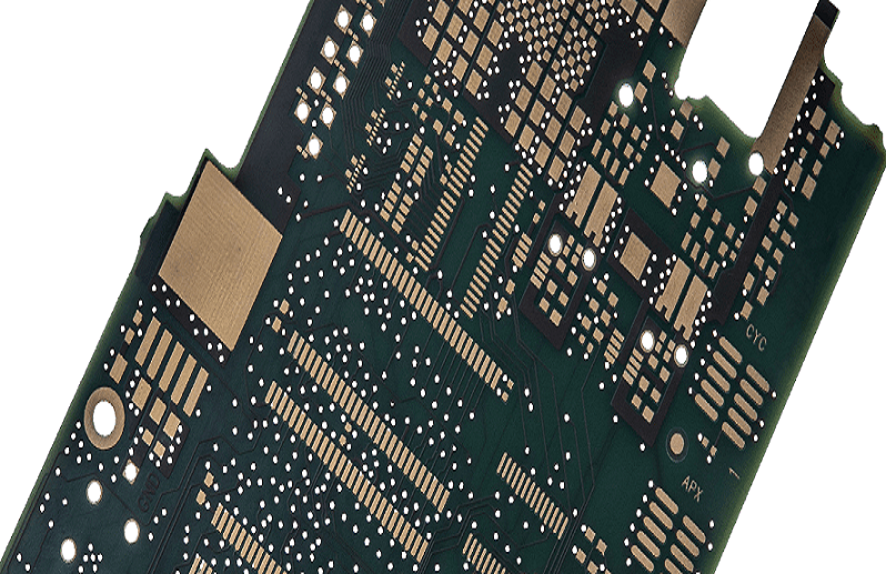
What is Ultra HDI PCB?
In production facilities, engineering teams regularly encounter designs that exceed the limits of standard high density interconnect (HDI) circuits. Fine-pitch BGAs, high-speed signal paths, and ultra-compact form factors create consistent challenges with yield, reliability, and dimensional stability. Procurement specialists manage cost and lead-time risks from improperly specified materials and processes, while designers balance miniaturization goals with real-world fabrication limits. Ultra HDI PCB represents the most advanced category of interconnect technology, built around ultra-fine features, specialized materials, and tightly controlled processes validated for volume manufacturing. This framework delivers extreme routing density while maintaining consistent quality in commercial and industrial production environments.
Learn more about: Ultra HDI PCB Manufacturing Capabilities & Design
Ultra-fine Trace Width and Spacing
Dimensional Standards and Tolerances
Ultra HDI circuits rely on trace geometries that push established manufacturing limits, with strict numerical values for stable production. Standard trace width and spacing start at 30μm/30μm, with advanced processes supporting dimensions as small as 15μm/15μm for specialized high-density layouts. Tolerance limits are held to ±5μm for traces above 30μm and ±3μm for features below 30μm, following IPC-2226 Level C+ specifications. Impedance control uses calibrated dielectric thickness and trace sizing, with 50Ω single-ended and 100Ω differential profiles configured for each material stackup.
Process Comparisons and Quality Rules
Two critical process comparisons determine manufacturability and performance at Ultra HDI scales. The modified semi-additive process (mSAP) creates vertical sidewalls and high dimensional stability for traces below 30μm, while conventional subtractive etching produces undercut and line-edge roughness that increases scrap rates. Laser Direct Imaging (LDI) maintains registration accuracy within 5μm, while traditional photolithography fails to resolve features below 50μm consistently. Quality controls include 1μm resolution automated optical inspection, etch chemistry temperature fixed at 30±1°C, and spray pressure calibrated between 1.5–2.0 bar to preserve profile geometry across all production panels.
Microvia Technology
Dimensions and Plating Requirements
Microvias form the core interconnect structure in Ultra HDI circuits, with fixed parameters to prevent failure and ensure long-term performance. Standard microvia diameters range from 50μm to 75μm, with high-precision capabilities down to 30μm for advanced build-up film substrates. Aspect ratio is strictly limited to 1:1 to support complete copper plating and eliminate void formation. Minimum plating thickness is set at 15μm, with void content controlled below 3% as verified by X-ray inspection and IPC-6016 standards. Each structure is validated after plating to remove weak connections before further processing.
Configuration Comparisons and Production Controls
Stacked and staggered via arrangements create measurable tradeoffs between routing efficiency and production yield. Stacked microvias increase routing density by approximately 25% but require full copper filling and precise layer alignment to maintain reliability. Staggered microvias improve yield by 8–10% in volume manufacturing but reduce usable routing space, making them preferred for applications where reliability takes priority over miniaturization. Production controls include vacuum-assisted filling systems and curing profiles at 175°C to reduce voids, along with 100% X-ray inspection to detect alignment shift and plating defects before assembly.
Advanced Materials
Core and Dielectric Selections
Material performance directly defines signal quality and thermal stability in Ultra HDI circuits, with specific grades matched to application demands. Core materials use high-Tg FR-4 (≥170°C) for commercial designs, with low-loss laminates including Rogers 4350B and Panasonic M7 for signal speeds above 25Gbps. Build-up layers use ABF or BT resin with dielectric thickness from 30μm to 50μm, selected for dimensional stability and laser drillability. Very Low Profile (VLP) copper foil with surface roughness below 0.3μm reduces high-frequency signal loss compared to standard copper materials.
Compatibility Comparisons and Processing Guidelines
Material mismatch represents a leading source of failure in Ultra HDI production, with clear comparisons guiding material selection. ABF build-up films maintain stability through multiple lamination cycles, while standard FR-4 materials experience significant dimensional shift after three or more press cycles. VLP copper foil reduces impedance variation to ±3%, while standard foil creates deviations above 10% in fine trace geometries. Processing rules include pre-baking at 120°C for 4 hours to reduce moisture below 0.1%, lamination at 180°C and 280psi for 90 minutes, and CTE matching within 3ppm/°C to prevent delamination during thermal cycling and reflow exposure.
Precision Manufacturing
Equipment and Process Windows
Ultra HDI fabrication requires specialized equipment with tightly defined operating windows to maintain repeatable quality. UV laser drilling systems provide 2μm positional accuracy for microvias, with speed profiles calibrated for core and build-up materials. Vacuum plating lines use pulse plating parameters to ensure uniform coverage in high-aspect structures. All critical operations take place in Class 10000 cleanrooms with temperature controlled at 22±1°C and humidity at 45±5% to minimize material movement and registration error during processing.
Inspection and Yield Management
Yield stability depends on layered inspection protocols and statistical process control. Automated optical inspection verifies trace dimensions and surface quality at 1μm resolution, while X-ray systems inspect microvia plating and fill quality for 100% of production panels. First-article inspection validates all critical dimensions before volume runs, with layer-by-layer checks to catch errors early and reduce scrap. Controlled parameters for etching, plating, and lamination reduce avoidable yield loss and improve consistency across production batches, with real-time adjustments triggered by out-of-specification measurements.
Factory Production Case Study
A 12-layer Ultra HDI circuit built for 5G wireless infrastructure uses a 2+8+2 stackup with 30μm/30μm traces, 50μm stacked microvias, and low-loss dielectric materials. Initial production showed microvia voiding above 7%, layer misalignment near 8μm, impedance variation over 10%, and warpage exceeding 0.7mm/m. Process corrections included improved vacuum filling, tighter laser registration, calibrated dielectric thickness, and symmetric copper balancing. After adjustments, void levels dropped below 2%, alignment improved to 3μm, impedance fell within ±4%, and warpage reached 0.3mm/m. Final production yield improved from 82% to 92%, with full qualification through thermal cycling and high-speed signal testing.
Common Design Errors in Production
Exceeding microvia aspect ratio beyond 1:1 consistently increases plating voids and early-life failures in field applications. Using standard FR-4 materials for signals above 10Gbps leads to excessive insertion loss and signal degradation that cannot be corrected in processing. Undersized traces without current rating create thermal rise and reliability risks in active circuit paths. Uncontrolled glass weave in dielectric materials introduces measurable impedance variation on high-speed signal layers. Traditional solder materials cannot resolve small Ultra HDI features, leading to bridging and insufficient coverage during assembly. Asymmetric stackup design without copper balancing drives warpage that disrupts surface mounting and long-term mechanical stability.
FAQ for Ultra HDI PCB
- What is the minimum trace width for mass-produced Ultra HDI?
The minimum stable trace width and spacing for volume Ultra HDI production is 30μm/30μm, with 15μm/15μm available for specialized high-cost applications requiring extreme miniaturization.
- How reliable are stacked microvias in Ultra HDI?
Stacked microvias provide improved routing density but require full copper filling and strict plating control to maintain reliability across thermal cycling profiles.
- Which materials work for medical/aerospace Ultra HDI?
Medical and aerospace applications typically use polyimide and ABF materials with high-temperature performance and biocompatibility profiles meeting industry regulatory requirements.
- How to control impedance in Ultra HDI with 30μm traces?
Impedance control in Ultra HDI relies on calibrated dielectric thickness, consistent trace dimensions, and pre-production simulation to maintain tight tolerance across all signal layers in volume production.


![Understanding PCB Costs & Pricing [Your Complete Guide]](https://hdicircuitboard.com/wp-content/uploads/elementor/thumbs/Understanding-PCB-Costs-Pricing-Your-Complete-Guide-qzzhe6mcaxuolkux3xalfktgavumi9y1aqfbs9bpv4.webp "Understanding PCB Costs & Pricing [Your Complete Guide]")


