
Blind Vias & Buried Vias in HDI PCBs: Key Differences & Use
Engineers designing high density interconnect PCBs and procurement teams sourcing them face persistent challenges in balancing routing density, signal integrity, and manufacturing cost—especially for fine-pitch component layouts and compact form factors. Traditional through-hole vias waste critical board space, create signal stubs that degrade high-speed performance, and limit the miniaturization possible with HDI circuit boards. Blind and buried vias solve these core issues by creating layer-specific electrical connections, a foundational technique for modern high density interconnect PCB design and production. This guide breaks down blind and buried vias from a factory engineer’s perspective, with actionable technical parameters, real manufacturing insights, and design best practices for high density interconnect PCBs of all complexities.
Learn more about: Minimum Trace Width, Spacing, and Microvia Size for High Density Interconnect (HDI) PCB Mass Production
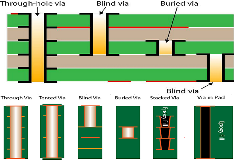
What Is a Blind Via?
Core Definition & IPC Classification
A blind via is a plated conductive hole in a high density interconnect PCB that connects a single outer layer (top or bottom) to one or more inner layers—without traversing the entire board thickness. Per IPC-A-600G (PCB inspection standards) and IPC-6016 (HDI PCB performance specifications), blind vias are classified as controlled-depth interconnects, with strict dimensional and plating requirements for compliance. Blind vias are visible from one outer board surface only, and their termination at specific inner layers eliminates unnecessary signal paths and frees up space on unconnected layers—an essential feature for HDI printed circuit boards with fine-pitch BGAs (≤0.8mm pitch) and compact footprints.
Critical Dimensional & Functional Specs
All blind vias in high density interconnect PCBs must meet factory-validated numerical specifications to ensure manufacturability and reliability, with no deviation for volume production:
- Diameter Range: 100μm (laser-drilled microvias) to 300μm (mechanically drilled) – IPC-6016
- Aspect Ratio: ≤1:1 (diameter:depth) for laser-drilled; ≤1.2:1 for mechanical (max for reliable plating)
- Plating Thickness: 20μm minimum barrel plating; 5μm minimum copper wrap on outer layer (IPC-6012 Class 2)
- Annular Ring: 90μm minimum (laser-drilled); 100μm minimum (mechanical) – prevents pad delamination
- Depth Tolerance: ±5μm for laser drilling; ±10μm for mechanical drilling (avoids over/under-drilling)
- Impedance Compatibility: Maintains 50Ω single-ended/100Ω differential impedance (±5% tolerance) for high-speed HDI boards
What Is a Buried Via?
Core Definition & IPC Classification
A buried via is a plated conductive hole in a high density interconnect PCB that connects two or more inner layers with no exposure to either outer board surface. Classified underIPC-A-600GandIPC-6016 as fully encapsulated interconnects, buried vias are entirely hidden within the HDI board’s layer stackup and are only accessible via cross-sectional inspection. This design eliminates any impact on outer layer component placement or trace routing, making buried vias indispensable for maximizing wiring density in complex high density interconnect PCB stackups (2+N+2 and higher).
Critical Dimensional & Functional Specs
Buried vias in high density interconnect PCBs have more stringent manufacturing specs than blind vias due to their fully encapsulated design, with all parameters aligned to IPC standards:
- Diameter Range: 150μm (laser-drilled) to 400μm (mechanically drilled) – IPC-6016
- Aspect Ratio: ≤1:10 (standard mechanical); ≤1:12 (special production) – IPC manufacturing guidelines
- Plating Thickness: 25μm minimum barrel plating (IPC-6012 Class 3) for high-reliability HDI boards
- Annular Ring: 90μm minimum (special production); 100μm minimum (standard) – inner layer pad stability
- Lamination Alignment: ±3μm between drilled vias and inner layer pads (prevents open circuits)
- Filling Requirement: 100% void-free epoxy/copper filling for vias in high-vibration HDI applications (automotive/aerospace)
Manufacturing Specifications
Drilling & Plating Processes
Blind and buried vias require specialized manufacturing processes distinct from through-hole vias, with each step tailored to high density interconnect PCB stackups and aligned to IPC standards—laser drilling is the primary method for HDI microvias (≤150μm):
- Laser Drilling (UV/CO₂): Used for blind/buried microvias in HDI printed circuit boards; achieves ±5μm positional accuracy, no resin smear, and smooth hole walls – critical for 1:1 aspect ratio plating
- UV lasers: Drill copper and dielectric in a single step (ideal for HDI build-up layers)
- CO₂ lasers: Faster drilling for larger vias; requires pre-etching of copper layers
- Mechanical Drilling (CNC): Used for larger blind/buried vias (≥200μm); requires controlled-depth bits and ±10μm positional accuracy – limited use in high-density HDI circuit boards
- Plating Process: Electroless copper plating (0.5–1μm) for hole seeding, followed by electrolytic copper plating (20–25μm) for barrel thickness; 100% coverage verified via 3D X-ray
- Lamination Integration:
- Blind vias: Drilled after final HDI board lamination (outer layer to inner layer)
- Buried vias: Drilled before final lamination (inner layer sub-stackups, then bonded to outer layers)
- Filling & Planarization: 100% void-free epoxy/copper filling (40–75psi vacuum pressure) for vias under fine-pitch components; chemical mechanical planarization (CMP) for ≤5μm surface flatness (HDI PCB requirement)
Quality Control & IPC Compliance Checks
Factory quality control for blind/buried vias in high density interconnect PCBs is rigorous, with in-process and final checks mandated by IPC standards to avoid costly rework and field failures—100% of HDI boards with these vias undergo the following:
- In-Process Checks: Real-time laser diameter measurement (±1μm); inline AOI for plating uniformity; lamination alignment verification (±3μm)
- Final Checks: 3D X-ray inspection for 0% voids in plating/filling; stylus profilometry for surface flatness; peel strength testing (≥6lb/in for copper plating); thermal cycling (-40°C to +125°C, 500 cycles) per IPC-TM-650
- Documentation: Full traceability of drill parameters, plating lot numbers, and inspection results – required for IPC-6016 Class 3 compliance (medical/aerospace HDI PCBs)
- Reject Criteria: Voids >5μm; plating thickness <20μm; annular ring <90μm; over-drilling into unconnected layers (all result in immediate scrap for high-density HDI circuit boards)
Performance Benefits for HDI PCBs
Technical Advantages Over Through-Hole Vias
Blind and buried vias outperform traditional through-hole vias in every key performance metric for high density interconnect PCBs, with quantifiable improvements that directly address engineer and procurement pain points—core benefits are amplified in HDI circuit boards with 4+ layers:
| Parameter | Blind/Buried Vias (HDI PCB) | Through-Hole Vias | Performance Improvement |
|---|---|---|---|
| Board Space Usage | 40–50% less surface/inner layer space | Full-board penetration (wastes 30–40% of space) | 30–40% smaller HDI PCB footprint |
| Parasitic Inductance | 50–100pH per via (no stubs) | 1–2nH per via (long signal stubs) | 20–30% lower signal noise |
| Routing Density | 120–160 pins/sq.in. | 40–80 pins/sq.in. | 2x higher component density on HDI boards |
| Signal Speed Support | Up to 50Gbps (high-speed HDI) | ≤10Gbps | Enables 5G/AI applications on HDI printed circuit boards |
| Thermal Dissipation | 10–15W/cm² (copper-filled vias) | 5–8W/cm² | 2x better heat removal for high-power ICs |
Cost & Design Benefits for HDI PCB Projects
While blind/buried vias add 15–20% to HDI PCB fabrication costs (specialized equipment/processes), they deliver net project cost savings by reducing overall design and production expenses for high density interconnect PCBs:
- Eliminates 1–2 layers from HDI stackups (e.g., 4-layer HDI with blind/buried vias = 6-layer through-hole HDI) – cuts material costs by 15–20%
- Reduces SMT placement errors by 30% (no via-related pad crowding) – lowers HDI board assembly rework costs
- Shortens design cycle time by 15–20% (simpler escape routing for fine-pitch BGAs) – faster time-to-market for HDI projects
- Improves volume production yield (92–96%) for HDI printed circuit boards – eliminates through-hole-related failures (e.g., trace shorting, pad delamination)
- Reduces field failure rates by 25% in high-vibration applications – no exposed via barrels to crack (critical for automotive/aerospace HDI PCBs)
Design & Application Considerations
HDI PCB Stackup & Design Rules
Engineers designing blind/buried vias for high density interconnect PCBs must align all decisions with manufacturing capabilities and IPC standards, with numerical rules for every design element to avoid DFM errors—non-negotiable for HDI circuit boards:
- Stackup Compatibility:
- Blind vias: Ideal for 1+N+1 HDI stackups (single build-up layer) – connect outer to inner layers only
- Buried vias: Required for 2+N+2 and higher HDI stackups – connect inner layer sub-stackups
- Via Placement:
- Blind vias: ≥2mm from HDI board edges (prevents delamination); ≤0.5mm from fine-pitch BGA pads (escape routing)
- Buried vias: No overlap with blind vias in layer stackup (avoids lamination stress – factory critical rule)
- Solder Mask Design: Solder mask dams ≥15μm between blind via pads (prevents soldering bridging on HDI PCBs); no solder mask on buried via inner layer pads
- Filling Requirements: Copper filling for blind vias under ≤0.4mm pitch BGAs (100% void-free); epoxy filling for buried vias (matches HDI laminate CTE ≤30ppm/°C)
- Impedance Calculation: Include via barrel/plating in HDI PCB impedance models – blind/buried vias add <2% impedance drift (IPC-6016 limit)
Industry-Specific Applications for HDI PCBs
Blind and buried vias are the foundation of high density interconnect PCB design across California’s leading tech industries, with application-specific specs tailored to performance and reliability requirements—all use cases leverage HDI’s miniaturization and density benefits:
- AI & Data Centers: 100μm laser-drilled blind vias in 36-layer HDI circuit boards; supports 50Gbps signal speeds and GPU thermal dissipation (15W/cm²)
- Consumer Electronics: 150μm blind/buried microvias in 4–6 layer HDI printed circuit boards; 40% smaller footprint for smartphones/wearables
- Medical Devices: IPC-6016 Class 3 buried vias in rigid-flex HDI PCBs; 100% copper filling and hermetic sealing for implantable/portable diagnostic devices
- Automotive ADAS: 200μm mechanically drilled blind vias in high-Tg HDI circuit boards (Tg ≥180°C); resistance to -40°C to +125°C thermal cycling
- Aerospace & Defense: 150μm laser-drilled buried vias in radiation-hardened HDI PCBs; ±3μm lamination alignment for extreme reliability
Real Factory HDI PCB Case Study
Project Overview & Initial Parameters
A California-based AI hardware manufacturer required an 8-layer 2+6+2 high density interconnect PCB for a edge computing module, with blind and buried vias for 0.5mm pitch BGAs and 25Gbps signal speeds—core specs:
- Blind Vias: 100μm laser-drilled (top/bottom to L2/L7), 1:1 aspect ratio, copper-filled, 90μm annular ring (IPC-6016)
- Buried Vias: 150μm laser-drilled (L3-L6), 1:10 aspect ratio, epoxy-filled, 90μm annular ring (special production)
- HDI PCB Specs: 30μm/30μm trace/space, 1.0mm thickness, low-loss dielectric (Df ≤0.008), 50Ω/100Ω impedance (±5% tolerance)
- Production Target: 100k units/year, yield ≥92%, 0 field failures for industrial AI applications
Manufacturing Challenges & Root Causes
Initial pilot production (10k units) of the high density interconnect PCB resulted in a 75% yield due to three blind/buried via-specific failures, all traceable to process parameter misalignment:
- Buried Via Lamination Misalignment (12% defects): ±8μm alignment error between inner layer sub-stackups – caused open circuits (IPC limit = ±3μm)
- Blind Via Plating Voids (10% defects): 40psi vacuum plating pressure (too low) – created 5–10μm voids in copper filling, leading to signal degradation
- Blind Via Over-Drilling (8% defects): Laser drill calibration set to ±8μm depth tolerance – drilled into unconnected inner layers (IPC limit = ±5μm)
Implemented Solutions & Quantified Results
The HDI PCB factory implemented three targeted process changes, all with numerical parameters, to resolve via failures and meet production targets for the high density interconnect board:
- Lamination Alignment Calibration: Upgraded to laser-guided lamination (±3μm accuracy) – eliminated buried via open circuits
- Vacuum Plating Optimization: Increased pressure to 75psi, ramped at 5psi/second – 100% void-free blind via plating (3D X-ray verified)
- Laser Drill Recalibration: Tightened depth tolerance to ±5μm, added real-time depth monitoring – no over-drilling in production
Final Production Results: 95% yield for the high density interconnect PCB, 0.3% rework rate, 0 field failures in 12 months of industrial use. Blind/buried via-related costs were reduced by 18% via volume production, and total HDI board project costs were 14% lower than the original through-hole via design (8-layer HDI vs. 10-layer through-hole PCB).
Common Design Errors
Blind Via Design Errors (HDI PCB Focus)
From a factory engineer perspective, 85% of blind via-related manufacturing failures in high density interconnect PCBs stem from avoidable design errors—all with clear numerical violations of IPC standards and HDI manufacturing capabilities:
- Exceeding Aspect Ratio: Designing 1:1.5 aspect ratio blind vias (IPC-6016 limit = 1:1) – causes uneven plating and open circuits (60% of blind via errors)
- Insufficient Annular Ring: <90μm annular ring for laser-drilled blind vias – leads to pad delamination during SMT (15% of errors)
- Unfilled Vias Under Fine-Pitch BGAs: Leaving blind vias unfilled for ≤0.5mm pitch components – causes solder wicking and poor joint formation (10% of errors)
- Via Placement Near HDI Board Edges: <2mm from edges – causes delamination during lamination/assembly (8% of errors)
- Overlapping Blind/Buried Vias: Stacking blind vias on top of buried vias – creates lamination stress and via barrel cracking (7% of errors)
Buried Via Design Errors
Buried via design errors in high density interconnect PCBs are less common but more costly to fix (requires HDI board rework of inner layers)—all are avoidable with factory-aligned design rules:
- Incorrect Lamination Timing: Designing buried vias for post-lamination drilling (must be pre-lamination) – impossible to manufacture (40% of buried via errors)
- Mismatched CTE for Filling Material: Epoxy CTE >35ppm/°C for FR-4 HDI PCBs – causes thermal stress and via barrel cracking (25% of errors)
- Smaller Diameter Than Aspect Ratio Allows: 100μm buried vias with 1:10 aspect ratio (minimum 150μm) – causes plating failure (20% of errors)
- Unverified Inner Layer Pad Alignment: <90μm pad-to-via alignment – leads to open circuits in lamination (15% of errors)
FAQ – Blind & Buried Vias for HDI PCB Design
1. When should I use a blind via vs. a buried via in an HDI PCB?
Use blind vias for high density interconnect PCBs with 1+N+1 stackups (single build-up layer) to connect outer layers to inner layers—ideal for fine-pitch BGA escape routing and compact consumer electronics HDI circuit boards. Use buried vias for 2+N+2 and higher HDI stackups to connect inner layer sub-stackups—required for complex AI/medical HDI printed circuit boards where outer layer space is critical for component placement.
2. What is the smallest laser-drilled blind/buried via for volume HDI PCB production?
The factory-validated smallest laser-drilled via for volume production (10k+ units) in high density interconnect PCBs is 100μm (blind)and150μm (buried). While 50μm microvias are technically possible for ultra-fine HDI designs, they increase production cost by 40–50% and reduce yield to 80–85%—not feasible for most volume HDI PCB projects.
3. How do blind/buried vias impact HDI PCB cost, and when are they cost-effective?
Blind/buried vias add 15–20% to the fabrication cost of a high density interconnect PCB for low-volume production (<10k units), but become cost-effective for volume production (100k+ units) (cost gap narrows to 5–10%) and for HDI circuit boards where they eliminate 1–2 layers (net cost savings of 15–20%). They are also cost-effective for fine-pitch BGAs (≤0.8mm) where through-hole vias are impossible—no alternative for these high density interconnect PCB designs.
4. Can blind/buried vias be used on rigid-flex HDI printed circuit boards?
Yes, with strict design rules: on rigid-flex HDI PCBs, blind vias are only allowed in rigid regions (≥2mm from flex-rigid transitions) and must be copper-filled (100% void-free). Buried vias are allowed in both rigid and flex inner layers but must use epoxy filling (matches flex material CTE ≤50ppm/°C) to avoid cracking during bending. Neither via type is allowed in flex outer layers—critical for rigid-flex high density interconnect PCB reliability.
If you need Blind Vias & Buried Vias PCB manufacturing or design support, our engineering team provides free DFM analysis.


![Understanding PCB Costs & Pricing [Your Complete Guide]](https://hdicircuitboard.com/wp-content/uploads/elementor/thumbs/Understanding-PCB-Costs-Pricing-Your-Complete-Guide-qzzhe6mcaxuolkux3xalfktgavumi9y1aqfbs9bpv4.webp "Understanding PCB Costs & Pricing [Your Complete Guide]")


