
Unpacking the Acronym: What PCB Really Means
PCB stands for Printed Circuit Board, a fundamental component in modern electronics that serves as both a mechanical support and electrical interconnection platform for electronic parts. Unlike outdated point-to-point wiring systems that were unreliable and bulky, the PCB circuit board transformed the electronics industry by standardizing component integration, reducing size, and boosting performance across devices.
At its core, a PCB circuit board consists of non-conductive substrate material with precisely etched or printed conductive pathways (traces) that facilitate signal flow between components like resistors, capacitors, transistors, and integrated circuits. This structure is the reason electronic devices have become smaller, more powerful, and more affordable over the decades, making PCBs indispensable in sectors from consumer tech to aerospace, medicine, and industrial automation.
The Anatomy of a PCB Circuit Board
Every PCB circuit board is constructed from layered materials, each with a specific function that contributes to overall performance, durability, and manufacturability. Understanding these layers is key to selecting the right PCB for any application.
Core Layers of a PCB Circuit Board
- Substrate: The base material, most commonly FR-4 (a fiberglass-epoxy composite), which provides structural rigidity and electrical insulation. FR-4 is preferred for its thermal stability, water resistance, and cost-effectiveness, while flexible printed circuit options use polyimide (PI) film to enable bendability.
- Copper Layer: A thin foil of copper (the primary conductive material) that forms the traces and pads. The number of copper layers classifies PCBs as single-sided, double-sided, or multilayer printed circuit boards, with thickness typically measured at 1oz per square foot (equivalent to 35 micrometers).
- Solder Mask: A non-conductive coating (usually green, though other colors are available) that covers copper traces to prevent short circuits, oxidation, and damage from environmental factors. It leaves pads and vias exposed to allow component soldering.
- Silkscreen: A top layer of ink that adds labels, symbols, logos, and component identifiers. This layer simplifies assembly, troubleshooting, and maintenance by clearly marking the function of each part of the board.
Critical Components: Blind Via and Via Technology
Vias are drilled holes that connect different copper layers in a PCB, and blind via technology is a game-changer for compact, high-density designs:
- Blind Via: Connects an outer copper layer to one or more inner layers without piercing the entire board, a key feature of hdi circuit boards that maximizes space efficiency.
- Through-Hole Via: Extends through the entire PCB, used in traditional designs for component mounting and interlayer connectivity.
- Buried Via: Connects only inner copper layers, eliminating surface clutter and enabling higher component density in multilayer printed circuit boards.
Types of PCB Circuit Boards: Matching Design to Application
Selecting the appropriate PCB type depends on factors like application complexity, space constraints, environmental conditions, and performance requirements. Below is a detailed breakdown of common PCB variants, including prototype circuit board options and specialized designs.
Classification by Layer Count
| Type | Key Characteristics | Common Uses | Industry Standard |
|---|---|---|---|
| Single-Sided | One copper layer; simple layout | Calculators, LED lights, basic remote controls | IPC-6012 Class 1 |
| Double-Sided | Two copper layers; vias for interconnection | Automotive dashboards, printers, LED lighting | IPC-6012 Class 2 |
| Multilayer Printed Circuit Board | Three or more copper layers; stacked structure | Laptops, server motherboards, 5G base stations, MRI machines | IPC-6012 Class 3 |
Classification by Flexibility
- Rigid PCB: Inflexible substrate (FR-4, metal core) offering high stability; used in TVs, desktop computers, industrial equipment, and automotive infotainment systems (complies with IPC-2221).
- Flexible Printed Circuit: Bendable polyimide substrate that adapts to tight spaces or movement; ideal for smartwatches, foldable phones, aerospace sensors, and camera modules (complies with IPC-2223).
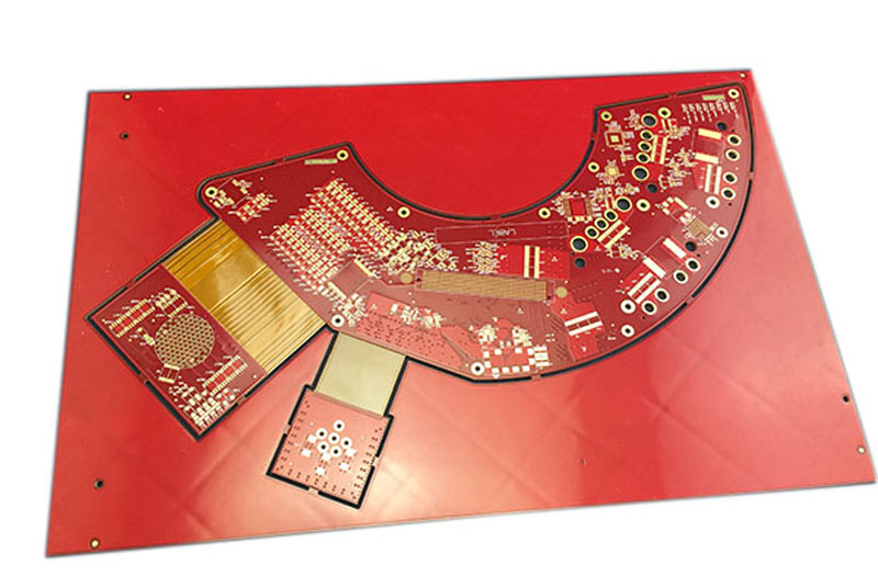
- Rigid-Flex PCB: Combines rigid and flexible sections for versatility; used in pacemakers, avionics, radar equipment, and laptop hinges (complies with IPC-2222).
Specialized PCB Types
- HDI Circuit Boards: High-Density Interconnect designs featuring microvias (≤100μm) and fine traces, optimized for compact devices like smartphones, medical implants, IoT devices, and wireless earbuds (complies with IPC-2226).
- RF PCB Design: Tailored for radio frequency applications with low dielectric loss materials (Teflon, Rogers) to maintain signal integrity; used in radar systems, telecommunications equipment, satellite devices, and GPS units (complies with IPC-2225).
- Prototype Circuit Board: Small-batch or custom-designed boards for product development and testing, available via traditional manufacturing or 3D printing for rapid iterations.
PCB Manufacturing: From Design to Finished Product
PCB manufacturing is a precise, multi-step process that converts digital designs into functional hardware, adhering to strict industry standards (such as IPC-6012 and IPC-2221) to ensure consistency and reliability.
Key Stages of PCB Manufacturing
- Schematic Design: Create a 2D blueprint using ECAD (Electronic Computer-Aided Design) software, mapping components, traces, and connections.
- Material Selection: Choose substrate (FR-4, polyimide, Rogers), copper thickness, and solder mask based on application requirements.
- Printing & Etching: Transfer the schematic to a copper-clad substrate, then etch away excess copper to reveal the desired traces and pads.
- Drilling: Precision-drill holes for through-holes, vias (including blind via), and component mounting.
- Plating: Coat drilled holes with copper to ensure electrical conductivity between layers.
- Solder Mask Application: Apply the protective solder mask layer, leaving critical areas (pads, vias) exposed.
- Silkscreen Printing: Add labels, logos, and component identifiers to the board’s surface.
- Testing & Inspection: Conduct automated tests (e.g., Design Rule Check/DRC) and visual inspections to detect defects like short circuits or misaligned vias.
Prototype Circuit Board Manufacturing
Prototype circuit board production prioritizes speed and cost-efficiency for design validation:
- Traditional methods: Small-batch etching and drilling, suitable for simple designs and quick iterations.
- 3D printing: Reduces production costs by up to 50% for custom prototypes, enabling rapid testing of unique layouts without expensive tooling.
PCB Design Essentials: Mastering RF, HDI, and Multilayer Designs
Effective PCB design is critical to performance, with specialized considerations for RF PCB design, hdi circuit boards, and multilayer printed circuit boards. Below are key best practices to address common challenges in design and manufacturing.
RF PCB Design Principles
RF PCB design requires meticulous attention to signal integrity and dielectric properties to minimize interference:
- Select low-loss materials (Rogers 4350B, Teflon) to maintain signal quality at frequencies above 1GHz.
- Optimize trace width and spacing to control impedance and reduce cross-talk between signals.
- Integrate ground planes and shielding to isolate RF signals from other components and external interference.
HDI Circuit Boards Design Tips
HDI circuit boards demand precision to maximize component density without sacrificing performance:
- Utilize blind via and microvia technology to connect layers without occupying surface space.
- Implement fine trace widths (≤100μm) and small pad sizes to accommodate compact components.
- Adhere to IPC-2226 standards for material selection, trace tolerances, and manufacturing processes.
Multilayer Printed Circuit Board Design Strategies
Multilayer printed circuit board design requires careful layer stacking and signal routing:
- Separate power and ground layers to reduce electrical noise and improve thermal management.
- Use prepreg (a dielectric material) to bond layers securely while maintaining insulation.
- Ensure alignment of vias (including blind via) across layers to guarantee consistent connectivity.
PCB vs. PCBA: Clearing Up Confusion
A common source of misunderstanding in electronics manufacturing is the difference between PCB and PCBA (Printed Circuit Board Assembly). Below is a detailed comparison to clarify their distinct roles.
| Aspect | PCB (Printed Circuit Board) | PCBA (Printed Circuit Board Assembly) |
|---|---|---|
| Definition | Blank board with conductive traces; no electronic components | PCB with all required components (resistors, ICs, sensors) installed |
| Functionality | Non-functional; requires assembly to operate | Fully functional; ready for integration into electronic devices |
| Manufacturing Process | Involves etching, drilling, layer lamination, and solder mask application | Adds component mounting via SMT (Surface-Mount Technology) or through-hole methods |
| Packaging | Vacuum-sealed to protect bare traces from damage | Anti-static or compartmental packaging to safeguard sensitive components |
| Cost | Lower; simpler production process with fewer steps | Higher; includes component costs, assembly labor, and quality control |
Frequently Asked Questions (FAQs) About PCB Circuit Boards
What Are the Primary Benefits of PCB Circuit Boards?
- Compact design: Enables smaller, more complex devices by replacing bulky wiring with etched traces.
- Reliability: Secure component mounting reduces loose connections and short circuits, improving device lifespan.
- Scalability: Ideal for mass production, with consistent quality and lower per-unit costs at high volumes.
- Low electrical noise: Component proximity and controlled trace routing minimize interference between signals.
- Reworkability: Design modifications are feasible using hot air rework stations, supporting iterative improvements.
How to Select the Right PCB Type for an Application?
- Evaluate complexity: Single-sided PCBs for simple devices, multilayer printed circuit boards for advanced electronics.
- Consider environmental factors: Flexible printed circuit for tight spaces or movement, rigid PCB for stability in harsh conditions.
- Assess frequency requirements: RF PCB design for high-frequency applications, standard materials for low-frequency use.
- Prioritize space constraints: HDI circuit boards or blind via technology for compact, high-density designs.
What Are the Key Industry Standards for PCB?
- IPC-6012: Specifies performance requirements for rigid PCBs, with three classes (1-3) for varying reliability needs (e.g., Class 3 for critical applications like medical devices).
- IPC-2221: Outlines general design requirements for rigid PCBs, including material selection, trace dimensions, and hole sizes.
- IPC-2223: Defines standards for flexible printed circuit design and manufacturing, covering material compatibility and bend radius.
- IPC-2226: Governs requirements for hdi circuit boards, including microvia specifications and trace tolerances.
The Future of PCB: Trends Shaping Manufacturing and Design
The PCB industry continues to evolve in response to demand for smaller, more powerful, and sustainable electronics. Key trends driving innovation include:
- Miniaturization: Further reduction in trace widths and component sizes, enabled by advances in hdi circuit boards and blind via technology.
- Flexible and stretchable materials: Expansion of flexible printed circuit applications in wearables, foldable devices, and medical implants.
- Transparent PCBs: Development of ceramic or glass-based substrates for see-through electronics like display panels and smart windows.
- Sustainable manufacturing: Adoption of eco-friendly materials and processes to reduce waste and environmental impact.
- Integration with emerging technologies: Support for 5G infrastructure, IoT devices, and electric vehicles, requiring advanced RF PCB design and multilayer printed circuit board solutions.
Conclusion
PCB stands for Printed Circuit Board, the unsung hero of modern electronics that enables the functionality of nearly every device we use. From prototype circuit board to high-performance RF PCB design, hdi circuit boards, and multilayer printed circuit boards, understanding the fundamentals of PCB types, structure, manufacturing, and design is essential for anyone involved in electronics development. By adhering to industry standards like IPC-6012 and IPC-2221, selecting the right materials and technologies (such as blind via and flexible printed circuit substrates), and following best practices for specialized designs, engineers and manufacturers can create PCBs that meet the demands of today’s most advanced applications. As technology continues to advance, PCBs will remain at the forefront of innovation, enabling smaller, faster, and more sustainable electronic devices for years to come. Whether you’re designing a simple consumer gadget or a complex aerospace system, the PCB circuit board is the foundation of reliable, efficient electronics.


![Understanding PCB Costs & Pricing [Your Complete Guide]](https://hdicircuitboard.com/wp-content/uploads/elementor/thumbs/Understanding-PCB-Costs-Pricing-Your-Complete-Guide-qzzhe6mcaxuolkux3xalfktgavumi9y1aqfbs9bpv4.webp "Understanding PCB Costs & Pricing [Your Complete Guide]")


