
A flexible printed circuit board is a lightweight, bendable interconnect system built on flexible polymer dielectrics, designed to support static shaping, dynamic bending, and 3D assembly while maintaining stable electrical performance. This guide provides fully actionable engineering data, manufacturing parameters, design rules, and reliability standards aligned with IPC‑2223, IPC‑6013, and UL requirements, supporting beginners and designers in selecting, specifying, and validating flexible PCB solutions for real-world production.
Learn more about: Flexible PCB: A Comprehensive Guide to Features, Applications, Types & Key Considerations
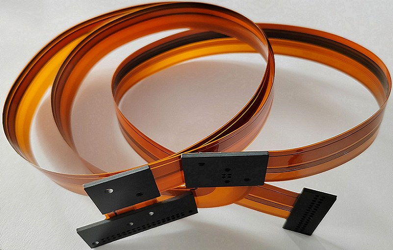
Definition and Core Function
A flexible PCB is a thin, conformable electrical circuit substrate that allows repeated bending, twisting, and installation into irregular enclosures. It replaces rigid FR‑4 boards and traditional wiring harnesses with higher reliability, smaller volume, and greater mechanical flexibility.
- Base thickness ranges from 25μm to 125μm for pure flex structures
- Supports operating temperatures from ‑40°C up to 150°C
- Delivers consistent conductivity under dynamic mechanical stress
- Reduces assembly steps and interconnect failure points
- Complies with IPC‑6013 for flex and rigid‑flex performance requirements
Key Aspects of Flexible PCBs
Structural Materials and Layer Composition
Every flexible PCB consists of engineered layers that define mechanical flexibility, thermal stability, and electrical behavior.
- Base dielectric: Polyimide (PI) in 25μm, 50μm, 75μm, and 125μm grades
- Conductor foil: Rolled Annealed (RA) copper for dynamic flex; Electrodeposited (ED) copper for static applications
- Bonding adhesive: 15μm to 25μm thermosetting epoxy or acrylic layers
- Coverlay: Protective polyimide film or liquid photo‑imageable solder mask
- Stiffener materials: FR‑4, aluminum, or PET for component mounting areas
Electrical and Mechanical Specifications
Standard manufacturing capabilities define reliable design boundaries for flexible PCB layouts.
- Minimum line and space: 50μm / 50μm for standard production; 30μm / 30μm for high‑precision HDI flex
- Minimum plated via diameter: 150μm for mechanical drilling; 75μm for laser microvias
- Impedance control: 50Ω, 90Ω, 100Ω with ±5% tolerance per IPC‑2223
- Bend radius: 2× substrate thickness for static flex; 5× to 10× thickness for dynamic flex
- Bending cycle life: 10,000 to 10,000,000 cycles based on copper type
Types of Flexible PCBs
Single‑Sided Flexible PCB
Single‑sided flex circuits include one conductive copper layer on a polyimide base.
- Total thickness: 50μm to 100μm
- Minimum trace width: 75μm
- No plated through‑vias required
- Ideal for low‑pin sensors, LED arrays, and simple signal interfaces
Double‑Sided Flexible PCB
Double‑sided flex includes two copper layers interconnected by plated through‑vias.
- Via diameter range: 150μm to 300μm
- Aspect ratio limited to 1:1 for consistent plating
- Supports 50μm / 50μm line and space capability
- Used in control interfaces, motor drivers, and compact interconnects
Multilayer Flexible PCB
Multilayer flex uses three or more copper layers with blind or buried vias for high routing density.
- Layer count: 3 to 12 layers
- Interlayer dielectric thickness: 40μm to 75μm
- Laser‑drilled microvias from 75μm to 125μm
- Applied in wearables, portable medical devices, and high‑density compact systems
Rigid‑Flex PCB
Rigid‑flex circuits integrate rigid FR‑4 regions and flexible polyimide zones in a single structure.
- Rigid sections for SMT and through‑hole components
- Flexible sections for 3D routing and folding
- Layer count from 4 to 30 layers
- Deployed in aerospace, automotive ADAS, and implantable medical electronics
Learn more about: What Is a Flexible Printed Circuit?
Advantages of Flexible Printed Circuit Boards
Space, Weight and Assembly Efficiency
- Reduces weight by 60% to 90% compared to conventional wiring harnesses
- Lowers overall assembly size by up to 70% in constrained enclosures
- Decreases component count and manual assembly labor
- Improves vibration and shock resistance in mobile environments
- Enables direct conforming to curved housing structures
Electrical Performance and Reliability
- Reduces parasitic inductance for improved high‑speed signal quality
- Maintains consistent impedance control in compact layouts
- Delivers strong resistance to humidity, thermal cycling, and chemical exposure
- Extends operational lifetime in dynamic flexing environments
- Minimizes open‑circuit and short‑circuit failure modes
Design Considerations for Flexible PCB
Trace Routing and Bending Geometry
- Route traces parallel to the bending axis to reduce mechanical stress
- Use curved traces with a minimum 1.5mm radius instead of sharp 90° angles
- Maintain minimum trace width of 150μm in dynamic flex zones
- Balance copper distribution to avoid warping and delamination
- Follow IPC‑2223 bend radius standards for long‑term reliability
Via, Clearance and Annular Ring Rules
- Minimum annular ring width: 75μm for all plated vias
- Minimum via‑to‑via spacing: 250μm to reduce stress concentration
- Minimum drill‑to‑copper clearance: 100μm on internal and external layers
- Avoid placing vias within dynamic bending zones
- Apply teardrop geometry at via‑trace junctions for improved strength
Stiffener and Component Placement
- Mount all SMT and through‑hole components on stiffened regions
- Stiffener thickness: 0.2mm to 1.0mm FR‑4 or aluminum
- Position connectors away from rigid‑flex transition areas
- Secure tall components with structural adhesive to prevent pad lift
Finishes and Colors in Flexible PCB Production
Standard Surface Finishes
- ENIG: Nickel 2–5μm, gold 0.05–0.1μm for corrosion stability
- ENEPIG: Includes palladium layer for fine‑pitch assembly reliability
- Immersion silver: Cost‑effective solderability for standard applications
- Soft gold: 0.3–1.0μm thickness for high‑cycle contact and dynamic interfaces
- Hot air solder level (HASL): Limited use due to flex surface stress
Coverlay and Silkscreen Appearance
- Standard coverlay: amber translucent polyimide
- Optional colors: black, white, green, blue
- Silkscreen ink: white or black for component identification
- Liquid photo‑imageable mask for fine‑feature definition and precision
Comparative Tables
RA Copper vs ED Copper for Flexible PCB
| Parameter | Rolled Annealed Copper | Electrodeposited Copper |
|---|---|---|
| Bending Cycles | 1,000,000+ | 10,000 – 100,000 |
| Elongation Rate | 25–30% | 10–15% |
| Relative Cost | 25–35% higher | Standard |
| Recommended Use | Dynamic flex zones | Static flex and rigid areas |
| Typical Thickness | 12μm, 18μm | 18μm, 35μm |
Single‑Sided vs Double‑Sided vs Multilayer Flex
| Structure | Layer Count | Minimum Line / Space | Cost Level | Typical Application |
|---|---|---|---|---|
| Single‑Sided Flex | 1 Layer | 75μm / 75μm | Low | Basic sensors & indicators |
| Double‑Sided Flex | 2 Layers | 50μm / 50μm | Medium | Control boards & interfaces |
| Multilayer Flex | 3–12 Layers | 30μm / 30μm | High | Wearables & high‑density electronics |
Technical Specifications
- Substrate thickness: 25μm – 125μm polyimide
- Copper foil thickness: 12μm – 35μm
- Minimum line / space: 30μm / 30μm (high precision), 50μm / 50μm (standard)
- Minimum via diameter: 75μm (laser), 150μm (mechanical)
- Bend radius: static = 2× thickness; dynamic = 5–10× thickness
- Impedance tolerance: ±5% per IPC‑2223
- Operating temperature: ‑40°C to 150°C
- Qualification standards: IPC‑6013, IPC‑2223, UL 94V‑0, RoHS
Case Study
Project Overview
Board type: 4‑layer rigid‑flex PCB with two rigid sections and one central flex zone; application: portable medical monitoring device; target bending cycles: 100,000; line / space: 75μm / 75μm.
Initial Manufacturing Issues
The original design used ED copper foil in the flex region, resulting in conductor cracking at 42,000 cycles. Traces routed perpendicular to the bend direction amplified stress. Insufficient coverlay margin caused edge peeling. Impedance deviation reached ±9%, outside acceptable tolerance.
Corrective Engineering Actions
Flex‑layer copper was changed to 18μm rolled annealed material. Traces were rerouted parallel to the bending axis. Coverlay margin was increased to 0.8mm. Trace geometry was adjusted to achieve impedance control within ±4.5%.
Final Production Results
Bending life exceeded 140,000 cycles without failure. Delamination and coverlay peeling were eliminated. Impedance stability measured at ±4.1%. Production yield improved from 74% to 95.3%. The design fully meets IPC‑6013 Class 2 performance requirements.
Common Design Errors
- Placing vias inside dynamic bending zones leads to early fracture and open circuits.
- Routing traces perpendicular to the bend direction increases stress by up to 500%.
- Using ED copper in dynamic flex applications causes fatigue and field failures.
- Insufficient coverlay margin below 0.5mm results in insulation breakdown and peeling.
- Asymmetric copper distribution causes substrate curling and lamination defects.
- Mounting components without stiffeners creates pad lifting and solder joint failure.
Quality Control and Reliability Testing
Factory Testing Procedures
- 100% electrical continuity and isolation testing
- TDR impedance verification for controlled impedance circuits
- Bending cycle validation to customer or industry specifications
- Thermal shock testing between ‑40°C and 125°C for 100 cycles
- Moisture resistance testing at 85°C and 85% RH over 168 hours
- Microsection analysis to verify plating quality and layer bonding
Industry Compliance Standards
- IPC‑2223: Design standard for flexible and rigid‑flex circuits
- IPC‑6013: Qualification and performance specification for flex PCBs
- IPC‑4101: Base material specifications for flexible dielectrics
- UL 746E: Safety standard for polyimide substrate materials
- ISO 9001, IATF 16949, RoHS, and REACH compliance
Frequently Asked Questions
Q1: What is the minimum bend radius for a flexible PCB?
A1: Static flex applications require a minimum bend radius of 2× the board thickness. Dynamic flex designs require 5× to 10× thickness as defined in IPC‑2223.
Q2: Which copper type is ideal for repeated dynamic bending?
A2: Rolled annealed (RA) copper offers superior ductility and supports more than one million bending cycles without conductor failure.
Q3: What is the difference between flexible PCB and rigid‑flex PCB?
A3: A flexible PCB is fully bendable across its entire area. A rigid‑flex PCB combines rigid sections for component mounting and flex sections for 3D routing and folding.
Q4: What is the standard finished thickness of a flexible PCB?
A4: Standard flexible PCBs without stiffeners range from 50μm to 125μm. Rigid‑flex assemblies typically range from 0.4mm to 2.0mm in total thickness.
If you need professional flexible PCB design support or quotation, our team provides free DFM check and fast turnaround.


![Understanding PCB Costs & Pricing [Your Complete Guide]](https://hdicircuitboard.com/wp-content/uploads/elementor/thumbs/Understanding-PCB-Costs-Pricing-Your-Complete-Guide-qzzhe6mcaxuolkux3xalfktgavumi9y1aqfbs9bpv4.webp "Understanding PCB Costs & Pricing [Your Complete Guide]")


