
What is a Microvia? Complete Guide to HDI PCB Microvia Types, Sizes & Manufacturing Standards
What is a HDI Microvia PCB?
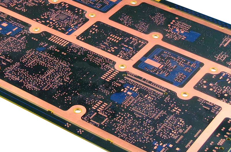
HDI Microvia PCB (High Density Interconnect Microvia Printed Circuit Board) is a specialized circuit board technology that integrates microvias to enable high-density routing, compact form factors, and enhanced signal integrity. These boards leverage microvia, blind via, and buried via structures to maximize interconnect density, making them ideal for applications like rigid flex pcb, flexible pcb, flexible printed circuit, rf pcb, and multilayer pcb designs where space constraints and performance are critical.
HDI Microvia PCB differs from standard multilayer pcb by using laser-drilled microvias (≤0.25mm diameter) instead of traditional mechanical through-holes, reducing via footprint by 50-70% and enabling finer lines & spaces (2-3mil). This technology complies with IPC-6012/2221 standards for HDI circuit boards, supporting sequential lamination processes to build complex layer stacks with stacked or staggered vias.
Key attributes of HDI Microvia PCB include:
- Integration of microvias (blind, buried, stacked, or staggered) for layer-to-layer connectivity
- Routing density 2-3x higher than standard PCB, supporting fine-pitch components (≤0.4mm BGA)
- Compatibility with flexible printed circuit and rigid flex pcb designs using polyimide substrates
- Enhanced signal integrity for rf pcb and high-speed applications (up to 100GHz) due to shorter via stubs
- Support for via-in-pad (VIP) and VIPPO (Via-in-Pad Plated Over) technologies to optimize component placement
HDI Microvia PCB is widely adopted in aerospace electronics, medical devices, smartphones, and automotive systems, where miniaturization and reliability are non-negotiable requirements for high density interconnect solutions.
Learn more about:How to Design HDI Microvia PCB
Microvia
A microvia is a miniature plated hole in a PCB or circuit board with a diameter of 0.25mm (10mil) or less, as defined by IPC-2221 standards. It is a foundational element of HDI pcb and high density interconnect designs, enabling compact layer-to-layer connectivity without the space requirements of traditional through-holes.
Microvias are laser-drilled, allowing for precise depth control and compatibility with thin dielectric materials (0.1-0.2mm) used in flexible pcb, rigid flex pcb, and multilayer pcb. Their small size reduces board thickness by 20-30% compared to standard PCBs, while supporting finer lines & spaces (2-3mil) for increased routing density.
Core characteristics of microvias include:
- Diameter range: 0.05mm (2mil) to 0.25mm (10mil)
- Aspect ratio (depth-to-diameter): Maximum 1:1 (per IPC-6012) for reliable plating
- Drilling method: UV or CO2 laser, with depth tolerance ±1mil
- Plating thickness: 15-25μm copper (electroless + electrolytic) to ensure conductivity
- Compatibility with sequential lamination processes for HDI circuit boards
Microvias address the challenge of routing dense I/O signals in fine-pitch components (e.g., 0.2mm BGA), enabling HDI pcb designs to support 2x more components per unit area than standard multilayer pcb. They are essential for flexible printed circuit and rf pcb applications, where space efficiency and signal integrity are critical.
Blind Microvias
Blind Microvias are a type of microvia that connects an outer layer of a PCB or circuit board to one or more inner layers without penetrating the entire board thickness. This design minimizes signal loss and crosstalk by reducing via stub length, making them ideal for high-speed and rf pcb applications in HDI circuit boards.
Blind Microvias are laser-drilled with precise depth control, ensuring they terminate exactly on target inner layers. They are commonly used in sequential lamination processes for multilayer pcb, rigid flex pcb, and flexible printed circuit, where space optimization and signal integrity are paramount.
Key specifications of Blind Microvias (per IPC-2221):
- Diameter: 0.05mm-0.25mm
- Depth: 0.1mm-0.5mm (limited by 1:1 aspect ratio)
- Plating: 15-25μm copper, with wrap-around onto surface pads (≥0.05mm overlap)
- Substrate compatibility: FR-4 (rigid), polyimide (flexible pcb), and low-loss materials (rf pcb)
Applications of Blind Microvias include:
- Fine-pitch BGA fanout routing in HDI pcb
- High-speed signal paths (≥10Gbps) in data center equipment
- RF PCB designs requiring controlled impedance (50Ω/90Ω)
- Flexible printed circuit and rigid flex pcb where through-holes would compromise flexibility
Blind Microvias reduce board weight and thickness while improving signal integrity by eliminating unused via stubs, a critical advantage for portable electronics and aerospace systems.
Buried Microvias
Buried Microvias are microvias that connect two or more inner layers of a multilayer pcb or HDI circuit board without reaching the outer layers. They are entirely encapsulated within the dielectric material, making them invisible from the board surface and enabling maximum routing density in high density interconnect designs.
Buried Microvias are fabricated during core lamination, using laser drilling before bonding inner layers. They comply with IPC-6012 standards for HDI pcb, supporting aspect ratios up to 1:1 and diameters as small as 0.05mm.
Key features of Buried Microvias:
- Connect only inner layers (no outer layer exposure)
- Diameter range: 0.05mm-0.25mm
- Depth: 0.1mm-0.5mm (1:1 aspect ratio)
- Plating: Electroless + electrolytic copper (15-25μm)
- Compatibility: Sequential lamination and standard multilayer pcb processes
Advantages of Buried Microvias for PCB design:
- Free up outer layer space for component placement and surface traces
- Reduce crosstalk between inner and outer layers in rf pcb
- Enable higher layer counts (16+ layers) in compact HDI circuit boards
- Support flexible printed circuit and rigid flex pcb by avoiding through-holes that weaken the substrate
Buried Microvias are critical for ultra-high-density HDI pcb designs, such as those used in medical imaging devices and high-performance computing, where maximizing routing density without compromising signal integrity is essential.
Stacked Vias
Stacked Vias are a series of microvias vertically aligned (stacked) to connect non-adjacent layers in a multilayer pcb or HDI circuit board. This configuration enables direct connectivity between outer layers and deep inner layers, eliminating the need for long trace routes and reducing signal delay.
Stacked Vias are fabricated using sequential lamination, with each microvia drilled and plated in a separate lamination cycle. They comply with IPC-4761 standards for via protection, requiring fill and planarization between cycles to ensure structural integrity.
Key specifications of Stacked Vias:
- Individual microvia diameter: 0.05mm-0.25mm
- Number of stacked layers: 2-4 (per IPC-6012)
- Aspect ratio per microvia: ≤1:1
- Total stack height: 0.2mm-1.0mm
- Fill type: Conductive (power) or non-conductive (signal) epoxy
Comparison of Stacked Vias vs. Traditional Vias:
| Parameter | Stacked Vias | Traditional Through-Holes |
|---|---|---|
| Space Requirement | 50-70% less | Larger footprint |
| Signal Delay | 30-40% lower | Higher due to longer traces |
| Board Thickness | Reduced by 20-30% | Thicker |
| Compatibility | HDI pcb, rigid flex pcb | Standard multilayer pcb |
| Cost | 20-30% higher | Lower |
Applications of Stacked Vias include:
- Fine-pitch BGA (≤0.3mm) fanout in HDI circuit boards
- High-speed data paths (≥25Gbps) in networking equipment
- Power distribution in compact rf pcb and flexible printed circuit
- Ultra-high-density designs (≥20 layers) in aerospace electronics
Stacked Vias enable HDI pcb designs to achieve 3x higher routing density than traditional PCBs, making them indispensable for miniaturized electronic devices.
Staggered Vias
Staggered Vias are microvias arranged in an offset (staggered) pattern to connect non-adjacent layers in a multilayer pcb or HDI circuit board. Unlike Stacked Vias, they do not share a vertical axis, reducing mechanical stress and improving manufacturability while maintaining high routing density.
Staggered Vias are laser-drilled and plated in sequential lamination cycles, with each microvia targeting a specific inner layer. They comply with IPC-2221 spacing requirements, with a minimum 0.2mm distance between adjacent microvias.
Key attributes of Staggered Vias:
- Individual microvia diameter: 0.05mm-0.25mm
- Offset distance between vias: ≥0.2mm (per IPC-2221)
- Aspect ratio per microvia: ≤1:1
- Layer connectivity: Non-adjacent inner layers or outer-to-inner layers
- Compatibility: Flexible pcb, rigid flex pcb, and rf pcb designs
Advantages of Staggered Vias over Stacked Vias:
- Lower mechanical stress (reduced risk of delamination in flexible printed circuit)
- Higher manufacturing yield (±0.1mil alignment tolerance vs. ±0.05mil for Stacked Vias)
- Better thermal dissipation in rf pcb and high-power applications
- Lower cost (fewer fill/planarization steps)
Applications of Staggered Vias:
- Mid-density HDI pcb (8-16 layers)
- Rigid flex pcb where bending stress is a concern
- RF PCB designs requiring thermal management
- Cost-sensitive high density interconnect applications
Staggered Vias balance routing density and manufacturability, making them a popular choice for HDI circuit boards in consumer electronics and industrial controls.
Microvia Size
Microvia Size is defined by two critical dimensions—diameter and depth—governed by IPC-2221 and IPC-6012 standards for HDI pcb and high density interconnect designs. These dimensions directly impact routing density, signal integrity, and manufacturability of PCB, circuit board, flexible pcb, and rigid flex pcb.
Diameter
Microvia Diameter refers to the hole size of the microvia, measured at the top surface of the dielectric layer. It is the primary factor determining routing density and compatibility with fine-pitch components.
Standard Microvia Diameter Ranges (per IPC-2221):
- Ultra-fine microvia: 0.05mm (2mil) to 0.10mm (4mil)
- Fine microvia: 0.10mm (4mil) to 0.15mm (6mil)
- Standard microvia: 0.15mm (6mil) to 0.25mm (10mil)
Diameter Selection Criteria:
- Component pitch: ≤0.3mm BGA requires ≤0.15mm microvias
- Routing density: Smaller diameters (0.05mm-0.10mm) enable 2x more vias per unit area
- Manufacturing capability: Ultra-fine microvias require UV laser drilling (higher cost)
- Signal type: RF PCB and high-speed signals (≥10Gbps) benefit from smaller diameters (reduced parasitic capacitance)
Depth
Microvia Depth is the distance from the top surface to the target layer, limited by the 1:1 aspect ratio (depth-to-diameter) per IPC-6012 standards to ensure reliable plating.
Standard Microvia Depth Ranges:
- Ultra-fine microvia (0.05mm-0.10mm diameter): 0.05mm-0.10mm depth
- Fine microvia (0.10mm-0.15mm diameter): 0.10mm-0.15mm depth
- Standard microvia (0.15mm-0.25mm diameter): 0.15mm-0.25mm depth
Depth Considerations for PCB Design:
- Dielectric thickness: Microvia depth must match the target layer’s dielectric thickness (±0.01mm)
- Layer connectivity: Blind microvias have depth equal to the distance from outer to inner layer
- Buried microvias have depth equal to the distance between two inner layers
- Flexible pcb and rigid flex pcb require shallower depths (≤0.15mm) to maintain flexibility
Microvia Size optimization balances routing density and manufacturability, with smaller diameters and depths enabling higher density but increasing fabrication complexity and cost.
VIPPO (Via-in-Pad Plated Over)
VIPPO (Via-in-Pad Plated Over) is a specialized microvia technology where a microvia is placed directly in a component pad, filled with conductive or non-conductive material, and plated over to create a flat surface. This design eliminates the need for dog-bone fanout, maximizing routing density and supporting fine-pitch components (≤0.3mm BGA) in HDI pcb and high density interconnect designs.
VIPPO complies with IPC-4761 standards for via protection, requiring precise fill and planarization to ensure solderability and component adhesion. It is compatible with flexible pcb, rigid flex pcb, rf pcb, and multilayer pcb, offering unique advantages for compact designs.
Key Specifications of VIPPO (per IPC-4761):
- Microvia diameter: 0.05mm-0.20mm
- Pad diameter: 0.20mm-0.50mm (4x microvia diameter minimum)
- Fill type: Conductive (epoxy + copper) or non-conductive (epoxy)
- Planarization tolerance: ±0.01mm (flatness)
- Plating thickness: 15-25μm copper (top surface)
Advantages of VIPPO for PCB Design:
- Eliminates fanout traces, increasing routing density by 30-40%
- Reduces signal delay (≤10ps) for high-speed paths in HDI circuit boards
- Supports fine-pitch components (≤0.2mm BGA) by utilizing pad space for vias
- Improves thermal dissipation in rf pcb and high-power applications (conductive fill)
- Enhances mechanical stability for flexible printed circuit and rigid flex pcb (no trace stress points)
Applications of VIPPO:
- Ultra-compact HDI pcb (e.g., wearables, medical sensors)
- Fine-pitch BGA and QFP components (≤0.3mm pitch)
- High-speed data paths (≥25Gbps) in networking equipment
- RF PCB designs requiring minimal signal loss
- Flexible pcb and rigid flex pcb where space is limited
VIPPO requires specialized manufacturing processes (fill, planarization, and precision plating), increasing cost by 15-20% compared to standard microvias, but delivers significant space and performance benefits for high-density designs.
Microvia Aspect Ratio
Microvia Aspect Ratio is the ratio of microvia depth to diameter, a critical parameter governed by IPC-6012 standards to ensure reliable copper plating and structural integrity. The maximum allowable aspect ratio for microvias is 1:1, meaning depth cannot exceed diameter, a key difference from traditional through-holes (aspect ratio up to 10:1).
Aspect Ratio Calculation & Standards
- Formula: Aspect Ratio = Microvia Depth / Microvia Diameter
- IPC-6012 Requirement: Maximum 1:1 for all microvias (blind, buried, stacked, staggered)
- Recommended Design Ratio: 0.8:1 to 1:1 (provides manufacturing tolerance)
Example Aspect Ratio Configurations:
- 0.10mm diameter microvia with 0.08mm depth: 0.8:1 (ideal)
- 0.15mm diameter microvia with 0.15mm depth: 1:1 (maximum allowed)
- 0.20mm diameter microvia with 0.25mm depth: 1.25:1 (non-compliant, risk of plating voids)
Impact on Manufacturing & Performance
- Plating Reliability: Aspect ratios exceeding 1:1 result in incomplete copper coverage (voids) due to limited electrolyte flow in narrow holes, leading to open circuits.
- Drilling Precision: Higher aspect ratios require more powerful lasers and slower drilling speeds, increasing cost and reducing yield.
- Signal Integrity: Lower aspect ratios (0.8:1) minimize parasitic capacitance and inductance, improving performance for rf pcb and high-speed signals (≥10Gbps).
- Flexibility: Flexible pcb and rigid flex pcb require aspect ratios ≤0.8:1 to prevent via cracking during bending.
Aspect Ratio Optimization for Different PCB Types
- HDI PCB: 0.9:1 to 1:1 (maximizes depth for layer connectivity while maintaining compliance)
- Flexible PCB/Flexible Printed Circuit: 0.7:1 to 0.8:1 (balances depth and flexibility)
- RF PCB: 0.8:1 (minimizes signal loss from parasitic elements)
- Rigid Flex PCB: 0.7:1 to 0.9:1 (accommodates both rigid and flexible sections)
Microvia Aspect Ratio compliance is non-negotiable for reliable HDI circuit board performance, with deviations from IPC-6


![Understanding PCB Costs & Pricing [Your Complete Guide]](https://hdicircuitboard.com/wp-content/uploads/elementor/thumbs/Understanding-PCB-Costs-Pricing-Your-Complete-Guide-qzzhe6mcaxuolkux3xalfktgavumi9y1aqfbs9bpv4.webp "Understanding PCB Costs & Pricing [Your Complete Guide]")


