
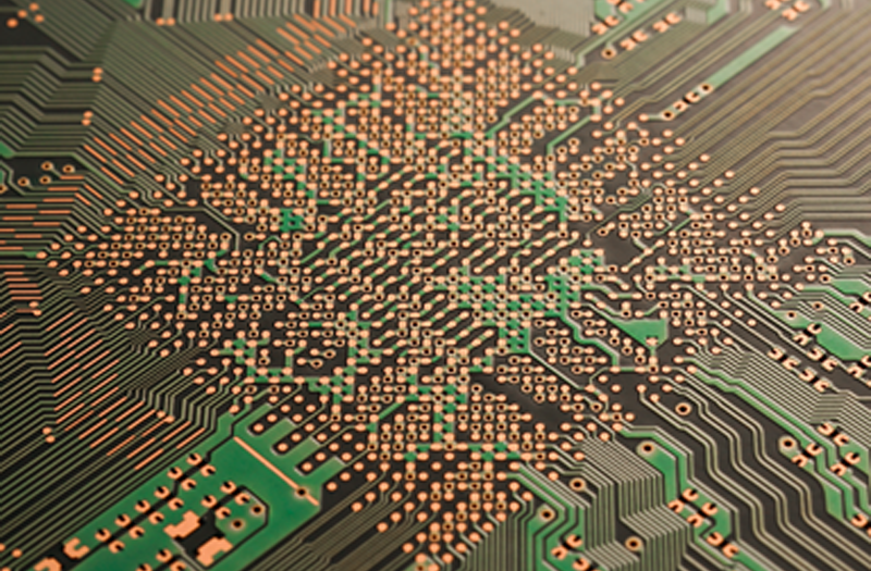
A printed circuit board (PCB) is a structured platform that mechanically supports electronic components and electrically connects them via conductive pathways etched onto non-conductive materials. Used in nearly every electronic device, PCBs replace messy point-to-point wiring with standardized, reliable designs that optimize performance, reduce size, and lower manufacturing costs. Below is a comprehensive breakdown of its core components, types, functions, and applications—aligned with industry standards like IPC-2221 and IPC-6012.
Core PCB Components: Layer by Layer Explanation
PCBs are constructed from alternating layers of conductive and non-conductive materials, each serving a critical role in functionality.
Substrate
- The base layer of a PCB, typically made from rigid fiberglass-reinforced epoxy (FR-4) for standard applications.
- Flexible PCBs use polyimide (PI) or polyester film as substrate, enabling bending and conforming to tight spaces.
- Key properties: Insulation, temperature stability (FR-4 withstands -40°C to 130°C), and mechanical rigidity.
- Industry standard: IPC-4101 specifies substrate material requirements for reliability.
- Application relevance: FR-4 substrates are ideal for household appliances and computers, while polyimide substrates excel in wearable tech and aerospace devices where flexibility is mandatory.
Copper Layers
- Thin copper foil laminated to the substrate, forming conductive “traces” that transmit electrical signals.
- Common thicknesses: 1oz (35µm) for standard use; 2–20oz for high-current applications (heavy copper PCBs).
- Configuration options:
- Single copper layer (for simple circuits)
- Dual copper layers (both sides of substrate)
- Multiple copper layers (separated by insulation in multilayer PCBs)
- Critical for signal integrity—thicker copper reduces resistance and heat buildup in power circuits.
- Application relevance: 1oz copper layers suit smartphones and radios, while 10oz+ copper is used in electric vehicle battery management systems and industrial motor controllers.
Solder Mask
- A non-conductive coating (typically green, but available in red, black, or white) applied over copper layers.
- Functions:
- Insulates traces to prevent short circuits from accidental solder contact.
- Protects copper from oxidation and environmental damage.
- Guides precise component soldering by exposing only pads and connectors.
- Compliance: IPC-SM-840 outlines solder mask material and application standards.
- Application relevance: Colored solder masks (e.g., black) are used in consumer electronics for aesthetic appeal, while high-temperature solder masks are mandatory for automotive under-hood components.
Silkscreen
- A printed layer (usually white) on top of the solder mask, featuring text, symbols, and component labels.
- Purpose:
- Simplifies assembly by identifying component positions (e.g., “R1” for resistor 1).
- Aids troubleshooting and maintenance with pin labels and polarity markers.
- Limitations: Low resolution—designs avoid fine details to ensure readability.
- Application relevance: Medical devices use silkscreen to mark sterilization indicators, while industrial PCBs include part numbers for quick replacement.
Vias
- Small holes drilled through the PCB to connect traces across layers.
- Types:
- Through-hole vias: Extend through the entire board (standard for double-sided/multilayer PCBs).
- Blind vias: Connect outer layers to inner layers (no penetration through the entire board).
- Buried vias: Connect inner layers only (hidden from outer surfaces).
- Microvia: Small vias (<150µm diameter) used in high density interconnect (HDI) PCBs for miniaturization.
- Critical for reducing board size in compact devices like smartphones and wearables.
- Application relevance: Microvias are essential in smartwatches and IoT sensors, while through-hole vias are preferred in industrial equipment for durability.
Key PCB Functions
PCBs serve three primary purposes that address core electronic design challenges:
Mechanical Support
- Secures components (resistors, capacitors, ICs) in fixed positions, preventing damage from vibration or movement.
- Rigid PCBs provide structural stability for devices like computer motherboards, while flexible PCBs offer support in dynamic environments (e.g., foldable phones).
- Eliminates the need for loose wiring, reducing component displacement and failure rates.
- Application example: Automotive dashboards use rigid PCBs to withstand road vibrations, while foldable phone hinges rely on flexible PCBs to maintain connectivity during bending.
Electrical Connections
- Copper traces act as dedicated pathways for power and data signals, ensuring consistent transmission between components.
- Reduces signal interference via controlled trace routing and layer separation (e.g., power layers isolated from signal layers).
- Enables complex circuit designs by organizing connections in a compact, predictable layout.
- Application example: 5G routers use multilayer PCBs with isolated signal layers to minimize interference, ensuring fast data transfer.
Efficiency & Size
- Consolidates multiple wiring paths into a single board, reducing device size by up to 70% compared to point-to-point wiring.
- Lowers manufacturing time with automated assembly (pick-and-place machines) and standardized designs.
- Improves energy efficiency by minimizing trace resistance, reducing power loss and heat generation.
- Application example: Wireless earbuds use HDI PCBs to fit complex circuitry into tiny enclosures, while electric vehicles rely on efficient PCB designs to extend battery life.
PCB Types: Classification & Use Cases
PCBs are categorized by structure, flexibility, and functionality to meet diverse application needs. Below is a detailed comparison:
| PCB Type | Key Features | Materials | Applications | Compliance Standard |
|---|---|---|---|---|
| Single-Sided | 1 copper layer; simple design | FR-4 | Calculators, LED lights, radios, basic remote controls | IPC-6012 Class 1 |
| Double-Sided | 2 copper layers; vias for interconnection | FR-4, polyimide | Mobile phones, routers, printers, automotive infotainment | IPC-6012 Class 2 |
| Multi-Layer | 3+ copper layers; stacked design | FR-4, Rogers | Laptops, server motherboards, MRI machines, 5G base stations | IPC-6012 Class 3 |
| Rigid | Inflexible substrate; high stability | FR-4, metal core | TVs, automotive dashboards, industrial equipment, desktop computers | IPC-2221 |
| Flexible (Flexible PCB/Flexible Printed Circuit) | Bendable polyimide substrate | Polyimide, PI film | Smartwatches, foldable phones, aerospace sensors, camera modules | IPC-2223 |
| Rigid-Flex (Rigid Flex PCB) | Combined rigid and flexible sections | FR-4 + polyimide | Pacemakers, radar equipment, avionics, laptop hinges | IPC-2222 |
| High Speed | Optimized for signal speeds >1GHz | Rogers 4350B, Teflon | 5G infrastructure, data centers, high-speed routers | IPC-2224 |
| RF PCB (Radio Frequency) | Low dielectric loss; high signal integrity | Teflon, Rogers | Radar systems, telecommunications, satellite equipment, GPS devices | IPC-2225 |
| HDI PCB (High Density Interconnect) | Microvias, fine traces (≤100µm) | FR-4, polyimide | Smartphones, medical implants, IoT devices, wireless earbuds | IPC-2226 |
Single-Sided PCB
- Simplest design with copper traces on one side of the substrate.
- Advantages: Low cost, easy manufacturing, fast assembly.
- Resolves: Budget constraints for basic electronics and low-volume production.
- Application deep dive: Used in disposable medical devices (e.g., glucose test strips) and entry-level consumer gadgets where functionality takes priority over complexity.
Double-Sided PCB
- Copper layers on both sides, connected via through-hole vias.
- Balances complexity and cost for mid-range devices.
- Resolves: Need for higher component density without the expense of multilayer PCBs.
- Application deep dive: Automotive LED lighting systems use double-sided PCBs to integrate power management and control circuits, while home routers rely on them for Wi-Fi and Ethernet connectivity.
Multi-Layer (Multilayer PCB)
- 3+ copper layers separated by insulation; up to 50 layers for advanced applications.
- Enables high component density and complex signal routing.
- Resolves: Space limitations in high-performance devices like graphics cards and aerospace systems.
- Application deep dive: Server motherboards use 16–24 layer PCBs to support multiple processors and memory modules, while MRI machines rely on 30+ layer designs for precise signal processing.
Rigid PCB
- Solid substrate (FR-4 or metal core) that maintains shape.
- Most widely used type; offers durability and easy testing.
- Resolves: Need for structural stability in static devices like home appliances and industrial machinery.
- Application deep dive: Refrigerator control panels use rigid PCBs to withstand temperature fluctuations, while industrial robots rely on them for precise motion control.
Flexible PCB (Flexible Printed Circuit/Flexible Circuit Board)
- Bendable, lightweight, and resistant to vibration.
- Reduces device weight by up to 30% compared to rigid PCBs.
- Resolves: Space constraints in curved or dynamic environments (wearables, camera modules, vehicle electronics).
- Application deep dive: Smartwatch straps integrate flexible PCBs to connect sensors and displays, while aerospace wiring harnesses use them to fit into tight fuselage spaces.
Rigid-Flex PCB
- Combines rigid sections (for component mounting) and flexible sections (for routing).
- Eliminates wiring harnesses, reducing assembly time and failure points.
- Resolves: Complex 3D layout needs in medical devices and aerospace navigation systems.
- Application deep dive: Pacemakers use rigid-flex PCBs to mount batteries (rigid section) and route signals around the heart (flexible section), while drone flight controllers rely on them for compact, vibration-resistant designs.
High Speed PCB
- Designed for signal speeds exceeding 1GHz with minimal loss.
- Uses low-dielectric materials (e.g., Rogers 4350B) to maintain signal integrity.
- Resolves: Signal degradation in 5G base stations and high-speed data processing.
- Application deep dive: 5G small cells use high-speed PCBs to handle 28GHz millimeter-wave signals, while data center switches rely on them for 100Gbps+ data transfer.
RF PCB
- Optimized for radio frequency signals (GHz range) with low interference.
- Features controlled impedance and shielding to minimize EMI.
- Resolves: Signal distortion in radar, satellite communication, and wireless chargers.
- Application deep dive: Satellite transceivers use RF PCBs to transmit signals through the atmosphere, while wireless charging pads rely on them for efficient power transfer at 13.56MHz.
PCB Manufacturing & Design Standards
Key Design Rules
- Trace width/spacing: ≥100µm for standard PCBs; 2/2mil (50/50µm) for HDI PCBs.
- Via size: ≥150µm for through-holes; 4mil (100µm) for microvias.
- Thermal relief: Required for pads connected to copper planes to ensure proper soldering.
- Design Rule Check (DRC): Mandatory to identify shorts, trace errors, or incompatible component placements.
- Application relevance: Medical device PCBs require stricter DRC checks to comply with FDA regulations, while automotive PCBs must meet AEC-Q200 standards for thermal and mechanical stress.
Manufacturing Process
- Schematic creation: 2D blueprint of components and connections using ECAD software.
- Material selection: Based on application (e.g., Teflon for RF PCBs, polyimide for flexible PCBs).
- Etching: Chemical removal of excess copper to form traces.
- Drilling: Creation of vias and component holes.
- Plating: Coating holes with copper to enable electrical connection between layers.
- Solder mask application: Insulating copper traces.
- Silkscreen printing: Adding labels and markers.
- Testing: Electrical and mechanical validation per IPC-6012.
- Application relevance: Aerospace PCBs undergo X-ray testing to detect hidden defects, while consumer electronics use automated optical inspection (AOI) for high-volume production.
Industry-Specific PCB Application Scenarios
Consumer Electronics
- Devices: Smartphones, laptops, wearables, wireless earbuds, gaming consoles.
- PCB Types: HDI PCBs, flexible PCBs, multilayer PCBs.
- Key Requirements: Miniaturization, low power consumption, aesthetic appeal.
- Example: iPhone motherboards use 10-layer HDI PCBs with microvias to fit 5G modems and processors into slim designs; Samsung Galaxy Z Fold series relies on flexible PCBs for foldable displays.
Automotive
- Devices: Electric vehicle (EV) battery management systems (BMS), infotainment systems, advanced driver-assistance systems (ADAS), LED headlights.
- PCB Types: Rigid PCBs, rigid-flex PCBs, heavy copper PCBs, metal core PCBs.
- Key Requirements: High temperature resistance (-40°C to 150°C), vibration resistance, long lifespan (15+ years).
- Example: Tesla Model 3 BMS uses heavy copper PCBs to handle 400V+ currents; ADAS cameras integrate rigid-flex PCBs to fit into windshield mounts.
Medical
- Devices: Pacemakers, MRI machines, glucose monitors, ultrasound probes, wearable health trackers.
- PCB Types: Rigid-flex PCBs, HDI PCBs, flexible PCBs.
- Key Requirements: Biocompatibility, miniaturization, reliability (failure rate <1 per million hours).
- Example: Implantable pacemakers use biocompatible rigid-flex PCBs; portable ultrasound probes rely on flexible PCBs to conform to body contours.
Aerospace & Defense
- Devices: Satellite transceivers, radar systems, avionics controls, military communication devices.
- PCB Types: RF PCBs, rigid-flex PCBs, multilayer PCBs.
- Key Requirements: Extreme temperature resistance (-55°C to 125°C), radiation resistance, shock resistance.
- Example: GPS satellites use RF PCBs to transmit signals through space; fighter jet avionics use rigid-flex PCBs to withstand high G-forces.
Industrial
- Devices: Motor controllers, programmable logic controllers (PLCs), industrial sensors, robotic arms.
- PCB Types: Rigid PCBs, heavy copper PCBs, metal core PCBs.
- Key Requirements: High voltage tolerance, dust/water resistance (IP67+), long-term stability.
- Example: Factory automation PLCs use rigid PCBs with thick copper traces; robotic arms integrate metal core PCBs for heat dissipation in high-load operations.
Telecommunications
- Devices: 5G base stations, routers, switches, satellite modems.
- PCB Types: High speed PCBs, RF PCBs, multilayer PCBs.
- Key Requirements: High signal integrity, low latency, high frequency support (up to 100GHz).
- Example: 5G macro base stations use high-speed PCBs for 3.5GHz mid-band signals; fiber optic switches rely on multilayer PCBs to route data between ports.
FAQ: Common PCB Questions
Q1: What’s the difference between a PCB and a PCA?
A: A PCB is the bare board (substrate + copper + solder mask + silkscreen). A PCA (Printed Circuit Assembly) is a PCB with mounted components (resistors, ICs, etc.).
Q2: How to choose the right PCB type for a project?
A: Evaluate three factors: 1) Space constraints (flexible/rigid-flex for tight areas), 2) Complexity (multilayer/HDI for dense components), 3) Environment (RF PCB for high-frequency needs, metal core for heat dissipation).
Q3: What is a microvia in HDI PCBs?
A: A microvia is a small via (<150µm diameter) used in high density interconnect PCBs to connect layers without occupying excessive space, enabling miniaturization.
Q4: Are flexible PCBs more reliable than rigid PCBs?
A: Flexible PCBs offer better vibration resistance but are more susceptible to physical damage if bent excessively. Rigid PCBs are more durable for static applications.
Q5: What standards ensure PCB quality for critical applications?
A: Medical PCBs comply with ISO 13485, automotive PCBs with IATF 16949, and aerospace PCBs with AS9100—all aligned with IPC core standards (IPC-2221, IPC-6012).
Key Takeaways
- PCBs are the foundation of modern electronics, offering mechanical support, electrical connection, and size efficiency across industries.
- Core components (substrate, copper layers, solder mask, silkscreen, vias) are tailored to application needs—from flexible substrates in wearables to heavy copper in EVs.
- Choosing the right type (single-sided, multilayer, flexible, rigid-flex, RF, HDI) depends on space, complexity, and environmental demands.
- Compliance with industry-specific standards (ISO 13485, IATF 16949, AS9100) and IPC benchmarks ensures reliability in critical applications.
By understanding these fundamentals, designers, manufacturers, and buyers can make informed decisions that optimize functionality, reduce costs, and ensure long-term reliability—whether for consumer gadgets, life-saving medical devices, or cutting-edge aerospace systems.


![Understanding PCB Costs & Pricing [Your Complete Guide]](https://hdicircuitboard.com/wp-content/uploads/elementor/thumbs/Understanding-PCB-Costs-Pricing-Your-Complete-Guide-qzzhe6mcaxuolkux3xalfktgavumi9y1aqfbs9bpv4.webp "Understanding PCB Costs & Pricing [Your Complete Guide]")


