
Defining Flexible PCB: Core Concepts & Key Specifications
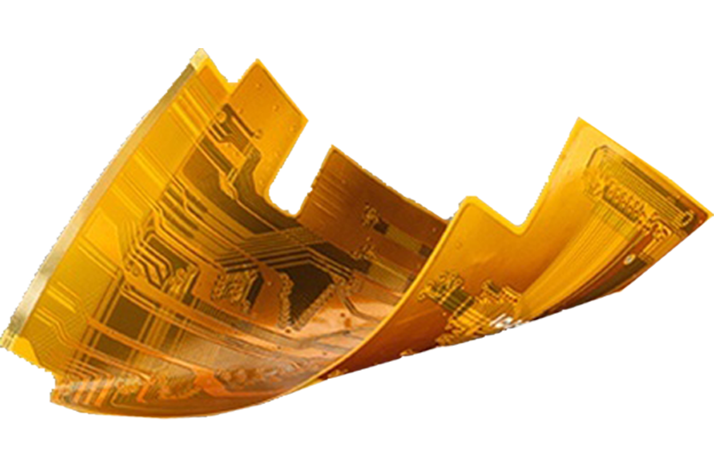
A flexible PCB (flexible printed circuit, flexible circuit board, or flexible printed circuit board) is an electronic interconnection solution built on pliable insulating substrates—primarily polyimide (PI) or polyester (PET)—that enables bending, folding, or twisting without compromising electrical performance. Unlike rigid PCBs, which rely on inflexible FR-4, the flexible printed circuit board is engineered to adapt to tight spaces, dynamic movements, and irregular form factors, making it indispensable in miniaturized and high-performance electronics.
Below are industry-standard performance specifications (aligned with IPC-2223) that validate its functionality across applications:
- Substrate thickness: 25–50μm (polyimide) or 100–250μm (PET), enabling overall board thickness as low as 0.1mm for single-layer designs.
- Copper layer options: 1/4oz (9μm) to 4oz (140μm), with a minimum elongation of 15% to resist fatigue during repeated bending.
- Operating temperature range: -40°C to 125°C (conventional); up to 300°C for high temperature flexible PCB variants.
- Bending durability: Withstands 100,000+ dynamic bending cycles (at a radius of 3x the board thickness) without trace cracking or insulation failure.
- Signal integrity: Maintains controlled impedance (50Ω–100Ω) for high-speed data transmission (up to 10Gbps) in aerospace and consumer electronics.
Types of Flexible PCB: From Standard to Specialized Variants
Flexible printed circuit boards are categorized by layer count, size, material, and specialized features, each tailored to address specific application challenges. Below is a detailed breakdown, including critical data and use cases.
Standard Flexible PCB Types (By Layer Count)
| Type | Key Specifications | Applications | Compliance Standard |
|---|---|---|---|
| Single sided flexible PCB | 1 copper layer (9–35μm); 0.1–0.2mm thickness; 0.3mm minimum bend radius | Wearable sensors, remote controls, basic IoT devices | IPC-2223 Class 1 |
| Double sided flex PCB | 2 copper layers; 0.2–0.4mm thickness; laser-drilled vias (≤100μm); 0.5mm minimum bend radius | Smartphones, camera modules, automotive infotainment | IPC-2223 Class 2 |
| Multilayer PCB (Flexible) | 3–16 copper layers; 0.4–1.2mm thickness; blind/buried vias; 1.0mm minimum bend radius | Medical implants, 5G transceivers, aerospace avionics | IPC-2223 Class 3 |
Specialized Flexible PCB Variants
- Large-format flexible pcb: Engineered for sizes up to 1000mm × 2000mm, with a weight reduction of 40–60% compared to rigid PCBs of equivalent area. Used in industrial control panels, large-format displays, and aerospace interiors, maintaining flexibility even at full scale.
- High temperature flexible PCB: Utilizes ceramic-reinforced polyimide substrates and high-temperature adhesives, with continuous operating temperatures up to 300°C and short-term resistance to 350°C. Ideal for automotive engine compartments, industrial furnaces, and satellite thermal control systems.
- Thick copper flexible PCB: Features copper layers ≥3oz (105μm) to handle current loads up to 50A and improve thermal conductivity (200–300 W/m·K). Deployed in electric vehicle (EV) battery management systems, power inverters, and industrial power supplies.
- Sculptured Flex Circuit (Sculptured Finger Circuit): A precision-engineered variant with contoured, “sculpted” conductive features—also known as Sculptured Finger Circuit—designed for exact-fit integration in complex assemblies. Below is a detailed deep dive into this specialized type.
Sculptured Flex Circuit (Sculptured Finger Circuit): Deep Dive
What Is a Sculptured Flex Circuit (Sculptured Finger Circuit)?
A Sculptured Flex Circuit—commonly referred to as Sculptured Finger Circuit—is a highly customized flexible printed circuit board distinguished by its precision-machined, contoured conductive elements (fingers) that extend beyond the substrate boundary. Unlike standard flexible PCBs, the Sculptured Flex Circuit (Sculptured Finger Circuit) eliminates the need for separate connectors, adapters, or jumpers by integrating “sculpted” contact points directly into the circuit design.
The term “Sculptured Finger Circuit” derives from the finger-like, contoured projections that serve as built-in connectors, ensuring a secure, low-profile interface with other components. These fingers are precision-machined using laser cutting or CNC routing to achieve tight tolerances (±0.05mm), making the Sculptured Flex Circuit (Sculptured Finger Circuit) ideal for applications where space is extremely limited or exact fitting is critical.
Key Features & Technical Specifications of Sculptured Flex Circuit
- Sculpted Finger Design: Contoured fingers with thicknesses ranging from 0.2mm to 1.0mm, tailored to mate with specific connectors or board interfaces. Fingers can be straight, angled, or curved to match complex assembly geometries.
- Material Composition: Core substrate (polyimide, 25–50μm) paired with thick copper layers (2–4oz, 70–140μm) for mechanical rigidity in the sculpted areas, while maintaining flexibility in the substrate body.
- Manufacturing Precision: Laser-machined features with edge smoothness ≤0.01mm to prevent stress concentration and ensure reliable mating. Etching processes achieve consistent finger width (0.3–1.0mm) and spacing (0.3–1.0mm).
- Environmental Resistance: Operates in temperatures ranging from -55°C to 150°C (compliant with IPC-6013), with resistance to moisture (IPX4 rating) and chemical exposure (engine oils, cleaning solvents).
- Reliability Metrics: Withstands 50,000+ mating cycles without contact degradation; insertion force controlled at 0.5–2.0N per finger to avoid damage to mating components.
Advantages of Sculptured Flex Circuit (Sculptured Finger Circuit)
- Eliminates Extra Components: The integrated sculpted fingers replace discrete connectors, reducing part count by 30–50% and eliminating potential failure points (e.g., loose connector pins).
- Space Efficiency: Reduces assembly volume by 20–40% compared to traditional “flex + connector” setups, critical for miniaturized devices like medical implants and avionics.
- Improved Reliability: One-piece design reduces assembly errors by 60% and improves vibration resistance (tested to 20g, 10–2000Hz) compared to connector-based solutions.
- Cost Savings: Lowers total assembly cost by 15–30% by eliminating connector procurement, inventory, and installation labor.
Applications of Sculptured Flex Circuit (Sculptured Finger Circuit)
- Aerospace & Defense: Used in avionics control panels, radar systems, and satellite communication modules, where the Sculptured Flex Circuit’s exact fit and vibration resistance ensure mission-critical reliability.
- Medical Devices: Integrated into minimally invasive surgical tools, pacemaker leads, and diagnostic equipment, where space constraints and biocompatibility (USP Class VI materials) are non-negotiable.
- Automotive: Deployed in EV battery packs, advanced driver-assistance systems (ADAS), and dashboard electronics, where the Sculptured Flex Circuit withstands temperature fluctuations and vibration.
- Industrial Robotics: Used in robotic arm joints and end-effectors, where the sculpted fingers provide a flexible yet secure connection for moving components.
Manufacturing Process of Flexible PCB (With Sculptured Flex Circuit Focus)
The production of flexible printed circuit boards involves specialized steps to preserve substrate flexibility while ensuring precision. For Sculptured Flex Circuit (Sculptured Finger Circuit), additional machining and quality control stages are integrated to achieve the sculpted features.
General Flexible PCB Manufacturing Stages
- Substrate Cutting: Precision-cut flexible substrates (polyimide/PET) to size, with edge straightness tolerance ±0.1mm.
- Copper Lamination: Bond copper foil to the substrate using adhesive (or direct lamination) at 120–150°C and 1–2MPa pressure.
- Photolithography: Apply photoresist, expose to UV light via a stencil, and develop to define trace patterns.
- Etching: Remove excess copper using ferric chloride or ammonium persulfate, achieving trace width tolerance ±0.02mm.
- Via Drilling: Laser-drill microvias (≤100μm) for double sided flex PCB and multilayer PCB variants.
- Plating: Plate vias and pads with nickel (5–10μm) and gold (0.05–0.1μm) for corrosion resistance and solderability.
- Coverlay Application: Apply protective polyimide coverlay, aligning with pads/fingers to ensure exposure.
- Stiffener Attachment: Bond stiffeners (FR-4/aluminum) to component mounting areas, curing at 130–160°C.
Specialized Manufacturing for Sculptured Flex Circuit
- Finger Sculpting: After etching, use laser cutting or CNC routing to shape the sculpted fingers, achieving contour precision ±0.05mm.
- Deburring: Remove burrs from sculpted edges using plasma cleaning or abrasive finishing to ensure smooth mating.
- Dimensional Inspection: Use optical measurement systems (accuracy ±0.01mm) to verify finger geometry and spacing.
- Mating Testing: Conduct insertion/extraction tests (50,000 cycles) to validate contact reliability and insertion force consistency.
Design Considerations for Flexible PCB (Including Sculptured Flex Circuit)
Effective flexible printed circuit board design requires balancing electrical performance, mechanical flexibility, and manufacturability. For specialized variants like Sculptured Flex Circuit (Sculptured Finger Circuit), additional design constraints apply.
General Design Best Practices
- Bend Radius: Adhere to IPC-2223 standards (minimum radius = 3x board thickness for static bending, 10x for dynamic bending).
- Trace Routing: Use curved traces (not right angles) to distribute stress; avoid trace runs parallel to bend axes.
- Component Placement: Keep components ≥2mm away from bend lines; use stiffeners for heavy components (≥0.5g).
- Thermal Management: For thick copper flexible PCB and high temperature flexible PCB, incorporate thermal vias (density ≥10 vias/cm²) and heat sinks.
Sculptured Flex Circuit Design Guidelines
- Finger Geometry: Design fingers with smooth curves (radius ≥0.5mm) to avoid stress concentration; avoid sharp edges that could crack during bending.
- Material Matching: Ensure sculpted finger thickness matches mating component requirements (e.g., 0.5mm fingers for ZIF connectors).
- Substrate Support: Reinforce the area where fingers meet the substrate with a thin stiffener (0.1–0.2mm) to prevent tearing.
- Tolerance Stack-Up: Account for manufacturing tolerances (±0.05mm) when designing finger spacing to ensure proper mating.
Applications & Performance Data of Flexible PCB
Flexible printed circuit boards are deployed across industries, with performance data validating their effectiveness in diverse environments. Below are key application areas and quantifiable results.
Consumer Electronics
- Smartphones: Double sided flex PCB enables 30% thinner camera modules (0.8mm vs. 1.1mm with rigid PCBs) and 100,000+ hinge bends for foldable phones.
- Wearables: Single sided flexible PCB reduces device weight by 40% (e.g., 5g vs. 8.3g for smartwatch PCBs) while conforming to wrist contours.
- Large Displays: Large-format flexible pcb supports 65-inch curved displays with a bend radius of 500mm, reducing bezel size by 50%.
Automotive
- High Temperature Flexible PCB: Withstands 180°C in engine compartments for 10,000+ hours without performance degradation (tested per AEC-Q200).
- Thick Copper Flexible PCB: Reduces EV battery pack volume by 25% and improves heat dissipation by 30% compared to rigid copper busbars.
- Sculptured Flex Circuit: Cuts ADAS sensor assembly time by 40% and reduces failure rates from 2.3% to 0.5% (automotive industry data).
Aerospace & Medical
- Aerospace: High temperature flexible PCB operates at -55°C to 200°C in satellite systems, with 10-year reliability (per MIL-PRF-55110).
- Medical: Sculptured Flex Circuit (Sculptured Finger Circuit) enables 20% smaller minimally invasive surgical tools, with biocompatible materials meeting ISO 10993.
Flexible PCB vs. Rigid PCB: Data-Driven Comparison
| Metric | Flexible PCB (Including Sculptured Flex Circuit) | Rigid PCB |
|---|---|---|
| Weight (per cm²) | 0.2–0.5g | 1.0–1.5g |
| Thickness | 0.1–1.2mm | 1.6–6.0mm |
| Bending Capacity | 100,000+ cycles | 0 (inflexible) |
| Assembly Time | 30–50% faster (no wiring harnesses) | Slower (requires connectors/wiring) |
| Failure Rate (10-year) | 0.5–1.2% | 1.8–3.0% |
| Cost (per unit, 10k volume) | $2.50–$15.00 | $1.00–$8.00 |
FAQs About Flexible PCB & Sculptured Flex Circuit
What Makes Sculptured Flex Circuit Different From Standard Flexible PCBs?
Sculptured Flex Circuit (Sculptured Finger Circuit) integrates precision-machined, contoured fingers that act as built-in connectors, eliminating the need for separate components. Standard flexible PCBs require external connectors, adding size, cost, and potential failure points.
How to Select Between Single Sided Flexible PCB and Double Sided Flex PCB?
Choose single sided flexible PCB for simple, low-density designs (≤100 components) and cost sensitivity. Opt for double sided flex PCB for higher component density (100–500 components) and the need for interlayer connections via vias.
What Is the Maximum Size of Large-Format Flexible PCB?
Large-format flexible pcb can be manufactured up to 1000mm × 2000mm, with custom sizes available for specialized applications (e.g., aerospace interiors). Thicker substrates (≥100μm) are used for larger sizes to maintain structural integrity.
Can Sculptured Flex Circuit Be Used in Dynamic Bending Applications?
Yes—Sculptured Flex Circuit (Sculptured Finger Circuit) maintains flexibility in the substrate body, with the sculpted fingers designed to withstand dynamic bending (up to 10,000 cycles) when paired with proper bend radius design (≥5x substrate thickness).
Conclusion
Flexible PCB (flexible printed circuit) is a versatile, data-proven solution that transforms electronic design by enabling miniaturization, flexibility, and reliability. From standard Single sided flexible PCB and double sided flex PCB to specialized variants like large-format flexible pcb, high temperature flexible PCB, thick copper flexible PCB, and Sculptured Flex Circuit (Sculptured Finger Circuit), these boards address diverse application challenges across consumer electronics, automotive, aerospace, and medical industries.
The Sculptured Flex Circuit—also known as Sculptured Finger Circuit—stands out as a precision-engineered solution that eliminates extra components, reduces size, and improves reliability in complex assemblies. By adhering to industry standards (IPC-2223, IPC-6013) and leveraging specialized manufacturing processes, flexible printed circuit boards deliver quantifiable benefits: 30–60% weight reduction, 20–40% space savings, and 15–30% cost reduction compared to rigid PCBs. As technology advances, flexible PCB will continue to evolve, with innovations in materials (eco-friendly substrates), manufacturing (additive printing), and design (integrated sensors) expanding their potential. Whether you’re designing a foldable phone, an EV battery system, or a medical implant, understanding the technical specifications, types, and design guidelines of flexible PCB—including the specialized Sculptured Flex Circuit—ensures optimal performance and reliability.


![Understanding PCB Costs & Pricing [Your Complete Guide]](https://hdicircuitboard.com/wp-content/uploads/elementor/thumbs/Understanding-PCB-Costs-Pricing-Your-Complete-Guide-qzzhe6mcaxuolkux3xalfktgavumi9y1aqfbs9bpv4.webp "Understanding PCB Costs & Pricing [Your Complete Guide]")


