
What is HDI PCB? A Beginner’s Complete Engineering Guide
Electronics engineers and procurement professionals often struggle to balance component density, device size, and performance when selecting PCBs for modern devices. Traditional circuit boards fail to meet the miniaturization demands of smartphones, AI hardware, and medical devices, while also lacking the signal integrity needed for high-speed applications. High density interconnect (HDI) PCBs resolve these challenges by packing more functionality into smaller spaces without compromising reliability—but understanding their design, manufacturing, and application requires clarity on technical specifics and industry standards. This guide breaks down HDI PCBs from a factory engineer’s perspective, with actionable data and real-world insights for beginners.
Learn more about: How to Design HDI Microvia PCB
What is HDI PCB?
Core Definition & IPC Classification
High Density Interconnect (HDI) PCB is a advanced printed circuit board technology characterized by higher wiring density, smaller vias, and finer trace widths compared to conventional PCBs. Per IPC-2226, HDI PCBs are defined by:
- Trace widths/spacings ≤ 100μm (0.10mm)
- Microvias < 150μm in diameter
- Capture pads < 400μm (0.40mm)
- Connection pad density > 20 pads/cm²
IPC-2226 categorizes HDI PCBs into three types based on microvia and lamination structure:
- Type I: Single microvia layer on one/both core sides; blind vias only (no buried vias)
- Type II: Single microvia layer on one/both core sides; both blind and buried vias
- Type III: Two+ microvia layers on one/both core sides; stacked blind/buried vias
Evolution & Industry Significance
HDI technology emerged in the 1980s as a response to the need for smaller, more powerful electronics. The first sequential lamination HDI boards were produced in 1984, and today, the technology is critical to the growth of industries like AI, 5G, and medical devices. According to market projections, the global HDI PCB market is expected to reach $145.8 billion by 2027, with a 6.2% CAGR from 2023 to 2028—outpacing the overall PCB industry’s 5.4% growth rate. This expansion is driven by the rising demand for AI servers, which are projected to reach a $47 billion market size by 2026 (38.3% CAGR 2022-2026).
Key Features & Capabilities
Foundational Technical Parameters
HDI PCBs’ performance is defined by precise manufacturing specs that balance density and manufacturability:
- Microvia specifications: Laser-drilled microvias as small as 25μm (0.001”) with aspect ratio ≤ 1:1 (per IPC-6016)
- Trace dimensions: Fine lines/spaces as tight as 20μm/20μm (0.8mil/0.8mil) for advanced designs; 30μm/30μm (1.2mil/1.2mil) for standard production
- Layer configurations: Common stackups include 1+N+1 (single build-up layer) and 2+N+2 (two build-up layers); up to 36 layers for complex applications
- Copper weights: ⅓ oz (11.8μm) to 2 oz (70μm); ¼ oz standard for fine-line layers to minimize etching issues
- Impedance control: 50Ω single-ended and 100Ω differential impedance with ±5% tolerance (±2% for high-speed RF designs)
Core Functional Advantages
From a user perspective, HDI PCBs deliver four non-negotiable capabilities that solve real-world design constraints:
- Space efficiency: Replace 8-10 layer conventional PCBs with 4-6 layer HDI boards (50% layer reduction) while maintaining functionality
- Signal optimization: Shorten signal paths by 30-50% compared to traditional PCBs, reducing crosstalk and signal loss for 25Gbps+ data rates
- Thermal management: Copper-filled microvias and thermal via arrays improve heat dissipation by 20-30%, critical for high-power components
- Component compatibility: Support fine-pitch BGAs down to 0.2mm pitch, enabling integration of high-pin-count ICs in compact devices
Higher Wiring Density
Density-Driving Design Elements
HDI PCBs achieve superior wiring density through three key design innovations:
- Microvia technology: Laser-drilled microvias (25-150μm) occupy 70% less space than conventional through-holes (>200μm), allowing more interconnections per unit area
- Via-in-Pad (VIPPO): Vias placed directly within component pads (50-80μm diameter) eliminate the need for separate via landing areas, increasing routing density by 40%
- Any-Layer Interconnect (ELIC): All layers function as high-density layers, enabling direct connections between any two layers and 2-4x higher routing density than traditional stackups
Density Metrics & Real-World Impact
Wiring density is quantified by two key metrics that matter to engineers and procurement teams:
- Pins per square inch: HDI PCBs support 120-160 pins/sq.in. (vs. 40-80 pins/sq.in. for conventional PCBs)
- Traces per square inch: Advanced HDI designs achieve 200-300 traces/sq.in., compared to 80-120 traces/sq.in. for standard PCBs
This density translates to tangible benefits: a smartphone HDI PCB with ELIC structure packs 4x more functionality into a 50% smaller footprint than a conventional PCB, enabling the slim form factors of modern devices.
Miniaturization & Compact Design
Size Reduction Mechanisms
HDI PCBs enable miniaturization through four interconnected design and manufacturing strategies:
- Layer count optimization: A 6-layer HDI board delivers the same functionality as an 8-10 layer conventional PCB, reducing thickness by 30-40% (from 1.6mm to 0.8-1.0mm)
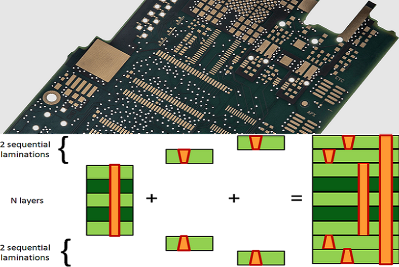
- Sequential lamination: Building layers one by one (instead of batch lamination) allows thinner dielectric layers (30μm vs. 100μm for conventional PCBs)
- Coreless construction: Eliminating rigid cores reduces board thickness to ≤0.4mm, ideal for wearables and flexible electronics
- Component placement efficiency: Blind/buried vias eliminate through-hole protrusions, enabling dual-sided component placement with 20-30% more components per unit area
Size Comparison & Practical Benefits
| Device Type | Conventional PCB Size | HDI PCB Size | Size Reduction |
|---|---|---|---|
| Smartphone Motherboard | 120x80mm (9600mm²) | 80x60mm (4800mm²) | 50% |
| Wearable Sensor Module | 40x30mm (1200mm²) | 25x20mm (500mm²) | 58% |
| Medical Implant PCB | 30x25mm (750mm²) | 20x18mm (360mm²) | 52% |
For engineers, this miniaturization means fitting complex electronics into space-constrained environments (e.g., automotive ADAS modules, hearing aids) without sacrificing performance. For procurement teams, smaller boards reduce material costs and shipping volumes, lowering total project expenses by 15-20%.
Superior Electrical Performance
Signal Integrity Enhancements
HDI PCBs outperform conventional PCBs in electrical performance due to design and material optimizations:
- Reduced signal path length: Shorter traces (average 50% shorter than conventional PCBs) minimize signal delay and attenuation, supporting data rates up to 50Gbps
- Minimized stubs: Blind/buried vias eliminate signal stubs (common in through-hole PCBs), reducing reflections by 60-70%
- Controlled impedance: Fine trace width control (±5μm) and low-loss materials (Dk 3.0-3.5) maintain impedance consistency, critical for DDR5 and PCIe 6.0 protocols
- Lower parasitic capacitance/inductance: Microvias have 1/10 the parasitic capacitance of through-holes, reducing noise and crosstalk
Material & Process Contributions
Electrical performance is further boosted by specialized materials and processes:
- High-Tg laminates: Tg ≥170°C materials (vs. 130°C for standard FR-4) maintain stability at high operating temperatures, preventing signal degradation
- Low-loss dielectrics: Materials like Rogers and modified FR-4 reduce dielectric loss (Df ≤0.008) for high-frequency applications (5G, RF)
- Laser direct imaging (LDI): 1μm resolution imaging ensures precise trace geometry, improving impedance control by 30% compared to traditional photolithography
Enhanced Thermal Management
Thermal Design Features
HDI PCBs address thermal challenges through targeted design elements:
- Copper-filled microvias: 100% void-free copper filling (per IPC-6016) provides thermal pathways, conducting heat 2x faster than unfilled vias
- Thermal via arrays: Dense arrays of 100μm thermal vias (100-200 vias/cm²) dissipate heat from high-power components (e.g., CPUs, FPGAs)
- Thick copper planes: 1-2 oz copper power/ground planes act as heat spreaders, reducing hotspots by 15-20°C
- Low-CTE materials: Dielectrics with Z-axis CTE ≤30ppm/°C minimize thermal stress between layers, preventing delamination
Thermal Performance Validation
Factory testing confirms HDI PCBs’ thermal superiority:
- Thermal cycling tests (-40°C to +125°C, 500 cycles) show no delamination or microvia cracking (per IPC-TM-650)
- Power dissipation testing: A 6-layer HDI PCB with thermal via arrays handles 15W/cm² vs. 8W/cm² for a conventional 8-layer PCB
- Real-world application: HDI PCBs in AI server GPUs reduce operating temperatures by 25-30°C compared to traditional designs, extending component lifespan by 30%
Advanced Manufacturing Technologies
Core Fabrication Processes
HDI PCB manufacturing requires specialized equipment and techniques not used in conventional PCB production:
- Laser drilling: UV/CO₂ lasers drill microvias at speeds up to 12,000 vias/second, with ±5μm positional accuracy (vs. ±20μm for mechanical drilling)
- Sequential lamination: Layer-by-layer lamination (2-7 cycles) enables thin dielectrics and precise layer alignment (±10μm registration)
- Modified Semi-Additive Process (mSAP): Creates fine traces (20μm) with rectangular profiles, improving current carrying capacity and signal integrity
- Vacuum via filling: Ensures 100% void-free filling of microvias with copper or epoxy, critical for thermal conductivity and mechanical stability
Quality Control & Standards Compliance
Manufacturing HDI PCBs requires rigorous quality control aligned with industry standards:
- In-process inspection: Automated Optical Inspection (AOI) with 1μm resolution checks trace width, spacing, and via quality
- X-ray inspection: 2D/3D X-ray verifies microvia filling (0% voids) and layer alignment
- Electrical testing: Flying probe testing (±2μm probe accuracy) validates continuity and impedance (±5% tolerance)
- Standard compliance: IPC-6016 (performance specs), IPC-2226 (design standards), and IPC-4104 (material requirements)
Broad Application Scope
Key Industry Applications
HDI PCBs are essential in industries demanding miniaturization, high performance, and reliability:
- Consumer electronics: Smartphones, wearables, tablets, and laptops (all modern smartphones use ELIC-structured HDI PCBs)
- AI & data centers: AI servers, GPUs, and high-speed networking equipment (HDI PCBs enable 25Gbps+ data rates)
- Automotive: ADAS modules, infotainment systems, and EV powertrain components (withstand -40°C to +125°C operating range)
- Medical devices: Pacemakers, diagnostic equipment, and wearable health monitors (biocompatible materials and miniaturized form factors)
- Aerospace & defense: Avionics, satellite communications, and military sensors (resist extreme temperatures and vibration)
Application-Specific Design Considerations
Each industry has unique requirements that shape HDI PCB design:
- Medical devices: Biocompatible surface finishes (ENIG), ultra-thin profiles (≤0.4mm), and 100% reliability testing
- Automotive: High-Tg materials (Tg ≥180°C), halogen-free laminates, and resistance to thermal cycling
- AI servers: Low-loss dielectrics, 50Ω/100Ω impedance control, and high layer counts (up to 36 layers)
HDI PCB vs. Conventional PCB – Critical Comparison
| Parameter | HDI PCB | Conventional PCB | User Advantage |
|---|---|---|---|
| Trace/Space | 20/20μm (advanced) | 100/100μm (standard) | 4x higher wiring density |
| Via Size | 25-150μm (microvias) | ≥200μm (through-holes) | 30-50% smaller board footprint |
| Layer Count | 4-6 layers (equivalent to 8-10 conventional) | 8-10 layers (same functionality) | 50% weight reduction |
| Signal Speed | Up to 50Gbps | ≤10Gbps | Enables high-speed AI/5G applications |
| Thermal Dissipation | 15W/cm² | 8W/cm² | Supports high-power components |
| Component Pitch | Down to 0.2mm | ≥0.8mm | Integrates high-pin-count ICs |
Real Factory HDI PCB Case Study
Project Overview & Initial Parameters
A consumer electronics manufacturer required a compact PCB for a wearable fitness tracker with:
- HDI Type: 1+4+1 stackup (Type II per IPC-2226)
- Key Specs: 30μm/30μm trace/space, 80μm microvias, 0.4mm BGA pitch, 0.6mm board thickness, high-Tg FR-4 (Tg 170°C)
- Production Target: 200k units/month, yield ≥92%
Manufacturing Challenges & Root Causes
Initial production runs (20k units) resulted in 76% yield due to three critical issues:
- Microvia voids (12% defects): Inadequate vacuum filling pressure (40psi) caused 5-10% voids in microvias
- Trace etching undercut (8% defects): Conventional subtractive process failed to maintain 30μm trace width (variation ±8μm)
- Layer misalignment (6% defects): Batch lamination caused ±15μm registration error between build-up layers
Implemented Solutions & Quantified Results
- Vacuum filling optimization: Increased pressure to 75psi, resulting in 100% void-free microvias (X-ray verified)
- Process switch to mSAP: Modified semi-additive process reduced trace width variation to ±3μm
- Sequential lamination adoption: Layer-by-layer lamination improved registration accuracy to ±8μm
Final Results: 94% production yield, 0.9% rework rate, 0 field failures in 12 months of consumer use. Material costs decreased by 18% due to layer count reduction (from 8 conventional layers to 6 HDI layers).
Common Design Errors (Production End Perspective)
- Exceeding microvia aspect ratio: Aspect ratio >1:1 (e.g., 150μm diameter × 200μm depth) causes uneven plating and voids (80% of microvia failures)
- Inadequate annular ring: <10μm annular ring for microvias leads to open circuits from drill wander (15μm minimum required)
- Asymmetric stackup design: Uneven copper distribution causes >0.75% warpage (IPC-6016 limit), leading to SMT placement failure
- Ignoring laser drilling constraints: Designing microvias <50μm for factories without UV laser capability (minimum 50μm for volume production)
- Poor solder mask design: <15μm solder mask dam between fine-pitch pads (0.4mm BGA) causes bridging (20μm minimum required)
- Unfilled vias under components: Unfilled microvias under BGAs/QFNs cause solder wicking and voids (assembly yield drop by 30%)
FAQ – HDI PCB Basics for Beginners
1. When should I choose an HDI PCB over a conventional PCB?
Choose HDI PCB if your design requires: component pitch ≤0.8mm, board size <100cm², signal speed >10Gbps, or layer count reduction (replace 8+ conventional layers with 4-6 HDI layers). For simple designs (component pitch ≥1.0mm, low signal speed), conventional PCBs are more cost-effective.
2. What is the minimum microvia size for volume production?
The minimum factory-validated microvia size for volume production is 50μm (laser-drilled). While 25μm microvias are possible for advanced applications, they increase production cost by 40-50% and reduce yield to 80-85%.
3. How do HDI PCB costs compare to conventional PCBs?
HDI PCBs have a 20-30% higher per-square-inch cost than conventional PCBs, but total project cost is often lower due to: 50% smaller board size, 30% fewer layers, and reduced assembly costs (dual-sided component placement). For high-volume production (100k+ units), the cost difference narrows to 10-15%.
4. What are the key design files needed for HDI PCB manufacturing?
Required files include: Gerber RS274X (all layers), ODB++ or IPC-2581 (design data), drill files (microvia and through-hole), layer stackup documentation (dielectric thickness, copper weight), impedance specifications, and DFM report (aligned with IPC-2226). If you need HDI PCB manufacturing or design support, our engineering team provides free DFM analysis and quotation.
Learn more about: Ultra HDI PCB Manufacturing Capabilities & Design


![Understanding PCB Costs & Pricing [Your Complete Guide]](https://hdicircuitboard.com/wp-content/uploads/elementor/thumbs/Understanding-PCB-Costs-Pricing-Your-Complete-Guide-qzzhe6mcaxuolkux3xalfktgavumi9y1aqfbs9bpv4.webp "Understanding PCB Costs & Pricing [Your Complete Guide]")


