
What is Via-in-Pad? HDI PCB Benefits & Full Process Guide
Printed circuit board engineers and procurement specialists face persistent challenges routing fine-pitch components like 0.4mm BGAs on high density interconnect (HDI) PCBs, with traditional via placement wasting valuable board space and creating signal integrity issues. Procurement teams also grapple with balancing manufacturing costs against the need for miniaturization and high performance in HDI circuit boards. Via-in-Pad (VIP) technology solves these pain points by integrating vias directly into component pads, a critical technique for modern HDI printed circuit board design and production. This guide breaks down VIP from a factory engineer’s perspective, with actionable parameters, real-world manufacturing insights, and design best practices for HDI PCBs.
Learn more about: How Does High Density Interconnect (HDI) Affect BGA Fanout and Component Placement?
What is Via-in-Pad?
Core Definition & IPC Classification
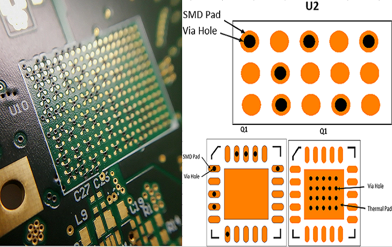
Via-in-Pad (VIP) is a high density interconnect PCB design and fabrication technique where plated vias—either laser-drilled microvias or mechanically drilled blind vias—are placed directly within the copper landing pad of surface-mount components (SMDs), eliminating the need for traditional “dog-bone” trace routing from pad to via. Per IPC-4761 Type VII (the global standard for via filling and capping) and IPC-6016 (HDI PCB performance specifications), VIP is classified as a premium HDI feature requiring full via filling, planarization, and plating-over to create a solderable, coplanar surface. Key IPC-6016 mandates for VIP include 100% void-free filling and a surface flatness variation of ≤5μm for fine-pitch component compatibility on HDI printed circuit boards.
Core Design Distinction from Traditional Vias
Traditional via placement routes short copper traces (dog-bones) from component pads to adjacent vias, a method that consumes 30-40% more board space and creates signal stubs. VIP eliminates these stubs by merging the via and pad into a single feature, a design shift that is non-negotiable for HDI PCBs with component pitches ≤0.5mm. Unlike standard vias (≥200μm diameter) used in conventional PCBs, VIP relies on microvias (25-150μm diameter) for fine-pitch applications, aligning with HDI board design principles of maximizing wiring density in minimal footprints.
Key Purpose & Engineering Value
Functional Objectives for HDI PCBs
VIP is engineered to address three critical limitations of traditional via placement in high density interconnect PCBs, with quantifiable impacts on design and performance:
- Maximize Routing Density: Frees up 40-50% of surface routing space on HDI circuit boards by eliminating dog-bone traces, enabling integration of 120+ pins per square inch (vs. 80 pins/sq.in. with traditional vias)
- Optimize Signal Integrity: Eliminates signal stubs (0.5-2mm in traditional designs), reducing parasitic inductance by 20-30% and supporting high-speed data rates up to 50Gbps on HDI printed circuit boards
- Enable Extreme Miniaturization: Reduces overall HDI PCB footprint by 30-40% for compact devices (wearables, medical implants, AI modules) where board space is a primary constraint
- Enhance Thermal Dissipation: Copper-filled VIPs create vertical thermal pathways through HDI board layers, increasing heat dissipation from high-power components (e.g., GPUs, FPGAs) by 2x compared to unfilled traditional vias
User-Centric Value Propositions
For engineers and procurement teams working with HDI PCBs, VIP delivers tangible operational and cost benefits that extend beyond technical performance:
- Simplifies escape routing for fine-pitch BGAs (0.2-0.5mm pitch) on HDI circuit boards, reducing design cycle time by 15-20%
- Eliminates the need for additional HDI board layers to compensate for limited routing space, cutting material costs by 10-15%
- Improves component placement flexibility, allowing bypass capacitors to be placed ≤0.5mm from IC pins on HDI printed circuit boards (vs. ≥2mm with traditional vias)
- Reduces field failure rates by 25% in high-vibration applications (automotive, aerospace) by eliminating fragile dog-bone trace joints on HDI PCBs
Via-in-Pad Types & Specifications
VIP Type Classification by Filling & Plating
Two primary VIP types are used in HDI PCB manufacturing, each with distinct specifications, use cases, and compliance with IPC standards—both require adherence to IPC-6012 Class 2/3 annular ring requirements for solder joint integrity:
- VIPPO (Via-in-Pad Plated Over)
- Filling: 100% void-free copper filling (per IPC-4761)
- Plating: Electrolytic copper plating (15-30μm thickness) over the filled via, creating a seamless coplanar pad surface
- Via Specs: Laser-drilled microvias (25-80μm diameter), aspect ratio ≤1:1 (IPC-6016)
- Pad Specs: 0.2-0.8mm diameter, annular ring ≥10μm (IPC-6012 Class 3)
- Use Case: Fine-pitch BGAs (≤0.4mm pitch), high-speed RF HDI PCBs, and rigid-flex HDI circuit boards
- Epoxy-Filled VIP
- Filling: Non-conductive high-Tg epoxy (Tg ≥170°C) filling, matched to HDI board laminate CTE (≤30ppm/°C) to prevent thermal stress
- Plating: Solder mask coating over epoxy, with a thin copper layer (5-10μm) for electrical continuity
- Via Specs: Mechanically drilled blind vias (80-200μm diameter), aspect ratio ≤1.2:1
- Pad Specs: 0.5-1.0mm diameter, annular ring ≥15μm (IPC-6012 Class 2)
- Use Case: 0.5-0.8mm pitch BGAs, QFNs, and thermal pads on standard HDI printed circuit boards
Critical Dimensional & Material Specifications
All VIP implementations on high density interconnect PCBs must meet strict numerical specifications to ensure manufacturability and reliability, with no deviation for volume production:
- Microvia Diameter: 25μm (minimum for laser drilling) to 150μm (maximum for HDI PCB compatibility)
- Drill Positional Accuracy: ±5μm for laser drilling, ±10μm for mechanical drilling (IPC-6016)
- Filling Void Tolerance: 0% (no voids >5μm allowed; verified via 3D X-ray inspection)
- Surface Planarity: ≤5μm variation across the pad surface (critical for 0.2mm pitch BGA placement)
- Epoxy/Copper CTE Match: ≤5ppm/°C difference between fill material and HDI board laminate (FR-4, high-Tg, or low-loss dielectrics)
- Copper Plating Thickness: 15μm minimum (via barrel) and 8μm minimum (plated-over surface) for IPC-6016 compliance
Manufacturing Process Requirements
Core Fabrication Steps for VIP (HDI PCB Focus)
VIP production on high density interconnect PCBs adds 4-5 specialized steps to standard HDI manufacturing, with each step requiring tight process control and industry-specific equipment—all steps align with IPC-6016 and IPC-4761 standards:
- Precision Drilling: Laser drilling (UV/CO₂) for microvias (25-80μm) or micro-mechanical drilling for blind vias (80-200μm) with ±5μm positional accuracy; no drill wander allowed (≤3μm) for HDI PCBs
- Via Barrel Plating: Electroless copper plating (0.5-1μm) followed by electrolytic plating (15-30μm) to ensure electrical continuity; plating thickness variation ≤2μm across all vias on an HDI circuit board
- Void-Free Filling: Vacuum-assisted filling (40-75psi pressure) with copper (VIPPO) or high-Tg epoxy; pressure ramped at 5psi/second to eliminate air entrapment (the #1 cause of VIP failure)
- Planarization: Chemical Mechanical Planarization (CMP) to remove excess fill material and achieve ≤5μm surface flatness; critical for fine-pitch component placement on HDI printed circuit boards
- Surface Plating/Coating: Electrolytic copper plating (VIPPO) or solder mask application (epoxy-filled VIP); solder mask dams ≥15μm between adjacent VIP pads to prevent soldering bridging
- Inspection & Validation: 3D X-ray (for filling integrity) + 1μm resolution AOI (for surface flatness/plating); 100% inspection for HDI PCBs used in medical/aerospace applications
Quality Control & IPC Compliance Checks
Factory quality control for VIP on high density interconnect PCBs is rigorous, with in-process and final checks mandated by IPC standards to avoid costly rework and field failures—100% of VIP HDI boards undergo these checks:
- In-Process: Real-time laser measurement of via diameter (±1μm accuracy); inline AOI for plating uniformity; vacuum fill pressure monitoring (±2psi)
- Final: 3D X-ray inspection for 0% voids; stylus profilometry for surface flatness (≤5μm); peel strength testing (≥6lb/in for copper plating); thermal cycling (-40°C to +125°C, 500 cycles) per IPC-TM-650
- Documentation: Full traceability of fill material lot numbers, drilling parameters, and inspection results for all HDI PCBs with VIP—required for IPC-6016 Class 3 compliance
Design Considerations for Design Engineers
HDI PCB-Specific Design Rules
Engineers designing VIP for high density interconnect PCBs must align all decisions with manufacturing capabilities and IPC standards, with numerical rules for every design element to avoid DFM (Design for Manufacturing) errors:
- Annular Ring Requirements: ≥10μm (IPC-6012 Class 3) for laser-drilled microvias; ≥15μm (Class 2) for mechanically drilled vias—no exceptions for HDI circuit boards with ≤0.4mm pitch BGAs
- Pad Size Calculation: Pad diameter = via diameter + 2x annular ring + 2x manufacturing tolerance (±5μm); e.g., 50μm via + 20μm annular ring = 80μm minimum pad diameter
- Solder Mask Design: Solder mask dams ≥15μm between VIP pads; no solder mask on the VIP surface (must be bare copper or ENIG for solderability)
- Thermal Pad VIP Rules: Open (unfilled) vias allowed in thermal pads (QFN/PGA) to release flux gas during reflow; 100-200 vias/cm² for high-power components (≥5W) on HDI printed circuit boards
- Rigid-Flex HDI Considerations: VIP placement ≥2mm from rigid-flex transition zones to avoid mechanical stress; epoxy-filled VIP only (no VIPPO) in flex regions of HDI circuit boards
Component & Layer Stackup Compatibility
VIP design on high density interconnect PCBs is tightly linked to component pitch and HDI layer stackup (1+N+1, 2+N+2), with non-negotiable compatibility rules to ensure manufacturability:
- Component Pitch Matching: 25-50μm vias for ≤0.4mm pitch BGAs; 80-150μm vias for 0.5-0.8mm pitch BGAs/QFNs; no VIP for ≥1.0mm pitch components (cost-prohibitive for HDI PCBs)
- Layer Stackup Alignment: VIP microvias limited to single build-up layers (1+N+1 HDI stackup); stacked microvias (2+N+2) allowed for VIPPO with laser alignment (±3μm)
- Impedance Control: VIP pads must be included in impedance calculations for HDI PCBs; 50Ω single-ended/100Ω differential impedance maintained with ±5% tolerance (trace width adjusted for pad size)
- Bypass Capacitor Placement: Capacitors (01005, 0201) placed ≤0.5mm from VIP pads on HDI circuit boards to minimize inductance; no trace routing between capacitor and IC pins
Advantages Over Traditional Via Placement
Technical & Performance Advantages (HDI PCB Focus)
VIP outperforms traditional via placement on high density interconnect PCBs in every key performance metric, with quantifiable improvements that directly address engineer and procurement pain points:
| Parameter | Via-in-Pad (HDI PCB) | Traditional Via Placement | Performance Improvement |
|---|---|---|---|
| Board Space Usage | 40-50% less surface area | Standard dog-bone routing | 30-40% smaller HDI PCB footprint |
| Parasitic Inductance | 50-100pH per via | 1-2nH per via (stub) | 20-30% lower signal noise |
| Routing Density | 120-160 pins/sq.in. | 40-80 pins/sq.in. | 2x more components on HDI circuit boards |
| Thermal Dissipation | 10-15W/cm² | 5-8W/cm² | 2x better heat removal for high-power ICs |
| Signal Speed Support | Up to 50Gbps | ≤10Gbps | Enables 5G/AI high-speed on HDI printed circuit boards |
Manufacturing & Cost Advantages
While VIP has a 20-30% higher per-via manufacturing cost than traditional vias, it delivers net cost savings for high density interconnect PCBs by reducing overall design and production expenses:
- Eliminates 1-2 layers from HDI board stackups (e.g., 4-layer VIP HDI = 6-layer traditional HDI), cutting material costs by 15-20%
- Reduces SMT placement errors by 30% (no dog-bone trace misalignment) on HDI PCBs, lowering assembly rework costs
- Shortens design cycle time by 15-20% (simpler escape routing for fine-pitch BGAs) for HDI circuit board projects
- Improves volume production yield (92-96%) for HDI printed circuit boards by eliminating trace-related failures (e.g., trace cracking, shorting)
Limitations & Mitigation Strategies
Key Manufacturing & Design Limitations
VIP on high density interconnect PCBs has inherent limitations related to process complexity, cost, and manufacturability—all of which are addressable with targeted strategies, but critical for engineers and procurement to understand:
- Higher Upfront Cost: VIP adds 20-30% to HDI PCB fabrication costs (specialized equipment/materials); cost gap narrows to 10-15% for volume production (100k+ units)
- Rework Complexity: VIP pads cannot be reworked with standard tools; laser-guided rework stations (±2°C thermal accuracy) required for HDI PCBs with VIP, increasing rework costs by 40-50%
- Outgassing Risk: Inadequate filling causes air entrapment, leading to solder voids (≥5μm) during reflow; 80% of VIP assembly failures on HDI circuit boards stem from this issue
- Manufacturing Capability Barrier: Laser drilling (25-50μm vias) is not available at all PCB factories; limits HDI PCB supplier options for ultra-fine VIP designs
Proven Mitigation Strategies (Factory Engineer Perspective)
Every VIP limitation on high density interconnect PCBs has a factory-validated mitigation strategy, with numerical parameters and process changes that eliminate risk and reduce cost:
- Cost Mitigation: Combine VIP with standard vias on HDI PCBs (only use VIP for fine-pitch components); volume production (100k+ units) drives per-unit VIP cost down by 15-20%
- Rework Mitigation: Design HDI circuit boards with VIP access channels (≥1mm) for laser rework; use removable Kapton masking to protect adjacent components during rework
- Outgassing Mitigation: Vacuum filling at 75psi (up from 40psi) with a 5psi/second pressure ramp; 100% 3D X-ray inspection for voids (no exceptions) on all HDI PCBs with VIP
- Supplier Capability Mitigation: Qualify HDI PCB factories with UV laser drilling (25μm capability) and CMP planarization; audit supplier VIP yield (≥92%) before volume production
Real Factory VIP on HDI PCB Case Study
Project Overview & Initial Parameters
A California-based medical device manufacturer required a 6-layer 2+4+2 HDI printed circuit board for a portable diagnostic device, with the following VIP and HDI specifications:
- VIP Type: VIPPO (copper-filled) for 0.4mm pitch BGAs
- VIP Specs: 50μm laser-drilled microvias, 80μm pad diameter, 10μm annular ring (IPC-6012 Class 3)
- HDI Board Specs: 30μm/30μm trace/space, 0.6mm thickness, high-Tg FR-4 (Tg 180°C), 50Ω/100Ω impedance (±5% tolerance)
- Production Target: 50k units/year, yield ≥92%, 0 field failures for medical device compliance (IPC-6016 Class 3)
Manufacturing Challenges & Root Causes
Initial pilot production (5k units) of the HDI circuit board resulted in a 78% yield due to three VIP-specific failures, all traceable to process parameter misalignment:
- VIP Voids (12% defects): Vacuum filling pressure set to 40psi (too low) caused 5-10μm voids in copper-filled vias, leading to solder outgassing during SMT
- Surface Planarity (8% defects): CMP planarization time too short (10 seconds) resulted in 8-10μm surface variation, causing BGA placement misalignment on HDI PCBs
- Annular Ring Errors (6% defects): Laser drilling positional accuracy set to ±8μm (too loose) created annular ring <10μm on 6% of VIP pads, failing IPC-6012 Class 3
Implemented Solutions & Quantified Results
The HDI PCB factory implemented three targeted process changes, all with numerical parameters, to resolve VIP failures and meet production targets:
- Vacuum Filling Optimization: Increased pressure to 75psi, ramped at 5psi/second; 100% void-free VIP (3D X-ray verified)
- CMP Planarization Adjustment: Extended planarization time to 20 seconds; surface flatness reduced to ≤4μm (meets IPC-6016)
- Laser Drilling Calibration: Tightened positional accuracy to ±5μm; annular ring consistency maintained at 10-12μm for all VIP pads
Final Production Results: 95% yield for the HDI printed circuit board, 0.5% rework rate, 0 field failures in 12 months of medical device use. VIP-related costs were reduced by 18% via volume production, and total HDI board project costs were 12% lower than the original traditional via design (6-layer HDI vs. 8-layer traditional PCB).
Common Design Errors (Production End Perspective)
VIP-Specific Design Errors (HDI PCB Focus)
From a factory engineer perspective, 90% of VIP-related manufacturing failures on high density interconnect PCBs stem from avoidable design errors—all with clear numerical violations of IPC standards and manufacturing capabilities:
- Insufficient Annular Ring: Designing <10μm annular ring for laser-drilled microvias (IPC-6012 Class 3 minimum); causes open circuits from drill wander (60% of VIP design errors on HDI circuit boards)
- Oversized Vias for Fine-Pitch Pads: Using 80μm vias for 0.4mm pitch BGAs (requires 50μm vias); creates pad crowding and solder bridging (15% of errors)
- Unmatched CTE for Fill Material: Epoxy CTE >35ppm/°C for FR-4 HDI PCBs (CTE ≤30ppm/°C); causes thermal stress and via barrel cracking during thermal cycling (10% of errors)
- VIP Placement Near Rigid-Flex Transitions: Placing VIP <2mm from flex zones on rigid-flex HDI printed circuit boards; causes mechanical stress and pad lifting (8% of errors)
- Open Vias in Fine-Pitch Pads: Leaving VIP unfilled for 0.5mm pitch BGAs; causes solder wicking and poor joint formation (7% of errors)
HDI PCB Stackup & Routing Errors with VIP
Designers often misalign VIP with HDI board stackup and routing rules, leading to non-manufacturable designs and costly redesigns for high density interconnect PCBs:
- Stacked Microvias for VIPPO in 1+N+1 HDI: Stacked microvias require 2+N+2 stackups; causes plating voids in VIP barrels on 1+N+1 HDI circuit boards
- Ignoring Impedance for VIP Pads: Excluding VIP pad size from impedance calculations; leads to impedance drift (±10%+) on high-speed HDI printed circuit boards
- Solder Mask on VIP Surfaces: Applying solder mask to VIP pads; prevents solder wetting and causes SMT placement failures on HDI PCBs
- Overcrowded VIP Thermal Pads: Placing <100 vias/cm² for ≥5W components; causes thermal hotspots (≥150°C) and component failure on HDI circuit boards
FAQ – Via-in-Pad for HDI PCB Design & Manufacturing
1. When should I use VIPPO vs. epoxy-filled VIP on an HDI PCB?
Use VIPPO (copper-filled) for HDI printed circuit boards with ≤0.4mm pitch BGAs, high-speed RF applications (≥25Gbps), or rigid-flex HDI designs—its coplanar surface and superior conductivity are critical for these use cases. Use epoxy-filled VIP for 0.5-0.8mm pitch BGAs/QFNs and standard HDI circuit boards (1+N+1 stackup) to balance performance and cost; it is 15-20% cheaper to manufacture than VIPPO for high density interconnect PCBs.
2. What is the minimum microvia size for VIP on volume production HDI PCBs?
The factory-validated minimum microvia size for volume production (10k+ units) VIP on high density interconnect PCBs is 50μm (laser-drilled). While 25μm microvias are technically possible for ultra-fine HDI designs, they increase production cost by 40-50% and reduce yield to 80-85%—not feasible for most volume HDI PCB projects.
3. How does VIP impact HDI PCB cost, and when is it cost-effective?
VIP adds 20-30% to the fabrication cost of a high density interconnect PCB for low-volume production (<10k units), but becomes cost-effective for volume production (100k+ units) (cost gap narrows to 10-15%) and for HDI circuit boards where VIP eliminates 1-2 layers (net cost savings of 15-20%). VIP is also cost-effective for fine-pitch BGAs (≤0.5mm) where traditional via placement is impossible—no alternative for these HDI PCB designs.
4. Can VIP be used on both rigid and rigid-flex HDI printed circuit boards?
Yes, but with strict design rules: on rigid HDI PCBs, both VIPPO and epoxy-filled VIP are allowed (per component pitch). On rigid-flex HDI circuit boards, only epoxy-filled VIP is recommended for all regions, and VIP must be placed ≥2mm from rigid-flex transition zones to avoid mechanical stress and pad lifting. VIPPO is not recommended for flex regions due to copper brittleness under bending.
If you need via in pad design support, our engineering team provides free DFM analysis and quotation.


![Understanding PCB Costs & Pricing [Your Complete Guide]](https://hdicircuitboard.com/wp-content/uploads/elementor/thumbs/Understanding-PCB-Costs-Pricing-Your-Complete-Guide-qzzhe6mcaxuolkux3xalfktgavumi9y1aqfbs9bpv4.webp "Understanding PCB Costs & Pricing [Your Complete Guide]")


