
high density interconnect (HDI) technology has become the backbone of modern electronics, enabling miniaturized, high-performance circuit boards that power everything from smartphones to aerospace systems. Defined by strict industry standards and specialized manufacturing techniques, HDI transforms how components connect by maximizing wiring density and minimizing signal loss. This guide breaks down HDI’s core principles, design fundamentals, and full manufacturing workflow—blending technical precision with practical utility for electronic engineers, PCB procurement professionals, and electronics enthusiasts.
Learn more about: How to Design HDI Microvia PCB
High-Density Interconnect Definition
HDI refers to advanced printed circuit board technology that achieves significantly higher wiring density per unit area than conventional PCBs, enabled by microvia structures, fine-pitch components, and sequential layer build-up.
Core Characteristics & IPC Standards
- IPC-2226 Definition: HDI is formally defined by IPC-2226 as boards with lines/spaces ≤100μm, vias ≤150μm, capture pads ≤400μm, and pad density >20 pads/cm².
- Key Traits: Compact form factor, reduced layer count (accomplishing the same functionality as traditional PCBs with 30-40% fewer layers), and enhanced Signal Integrity through shorter signal paths.
- Market Relevance: The global HDI market is projected to reach $39.91 billion by 2032 at a 12% CAGR, driven by demand for smaller, more powerful electronics.
HDI vs. Traditional PCB: Core Differences
| Aspect | HDI PCB | Traditional PCB |
|---|---|---|
| Wiring Density | 2-3x higher (supports fine-pitch BGAs ≤0.4mm) | Lower (limited to ≥0.8mm BGAs) |
| Via Technology | Microvias, blind vias, buried vias | Through-hole vias (≥12mil diameter) |
| Layer Efficiency | Fewer layers for equivalent functionality | More layers required for complex designs |
| Signal Integrity | Superior (shorter paths, reduced crosstalk) | Moderate (longer paths, higher parasitic effects) |
| Typical Applications | Wearables, medical devices, 5G infrastructure | Industrial controllers, basic consumer electronics |
HDI Design Basics
HDI design requires meticulous planning to balance density, manufacturability, and performance, with core principles centered on via technology, stack-up architecture, and material selection.
Core Structure Types of HDI
- 1+N+1 Stackup: One sequential lamination layer on each side of a central core (N), adding 2 copper layers (total N+2). Ideal for mid-density applications.
- 2+N+2 Stackup: Two sequential lamination layers on each side of the core, adding 4 copper layers (total N+4). Supports stacked microvias and high I/O density.
- ELIC (Every Layer Interconnect): All layers are freely interconnected via copper-filled stacked microvias, enabling maximum routing flexibility for complex, high-pin-count devices.
Design Rules for HDI
- Trace Width/Spacing: Standard HDI uses 50-75μm (2-3mil) trace width/spacing; advanced processes achieve 25-50μm (1-2mil) for ultra-high density.
- Annular Ring: Minimum 75μm (inner layers) and 100μm (outer layers) per IPC-2226 to prevent pad lifting or via breakout.
- Drill-to-Copper Clearance: 175-200μm (7-8mil) to avoid short circuits between vias and copper features.
Learn more about : How To Route HDI PCB
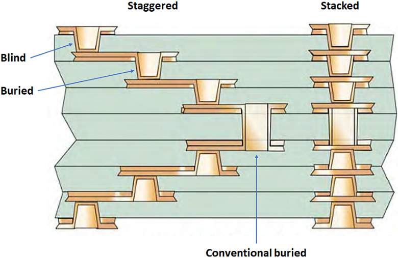
Microvias, Blind Vias, and Buried Vias
Via technology is the foundation of HDI, enabling dense layer-to-layer connectivity without sacrificing board size or performance.
Via Types & Functionalities
- Microvias: Laser-drilled vias with diameters ≤150μm (6mil), typically spanning 1-2 layers. Core to HDI density, as they occupy 60-70% less space than through-hole vias.
- Blind Vias: Connect outer layers to inner layers (e.g., Layer 1 to Layer 3) without penetrating the entire board, eliminating signal stubs that cause reflections.
- Buried Vias: Link inner layers exclusively (e.g., Layer 2 to Layer 4), preserving outer surface space for components and fine-pitch routing.
Minimum Microvia Size and Aspect Ratio
- Size Range: Standard microvias 100-150μm (4-6mil); advanced processes achieve 75-100μm (3-4mil) for ultra-dense designs.
- Aspect Ratio: Maximum 1:1 (depth-to-diameter) per IPC-2226 to ensure uniform copper plating. For a 100μm dielectric thickness, microvia diameter must be ≥100μm.
- Reliability Factor: Aspect ratio >1:1 increases plating defects (e.g., voids, thin copper) by 40-50%, reducing board lifespan.
Via-in-Pad (VIP) Design
Via-in-Pad integrates vias directly within component pads, a critical technique for maximizing HDI density and Signal Integrity.
VIP Design Principles & Specifications
- Pad Dimensions: VIP pads are 20-30% larger than microvia diameter (e.g., 250μm pad for 150μm microvia) to ensure full coverage and solderability.
- Filling Requirements: Vias are filled with conductive epoxy (power pins) or non-conductive epoxy (signal pins) and planarized to maintain pad flatness for SMT assembly.
- Offset Placement: Vias placed off-center (not in pad center) to prevent air entrapment during reflow soldering, which causes solder voids.
VIP vs. Traditional Adjacent Vias
| Aspect | Via-in-Pad (VIP) | Adjacent Via |
|---|---|---|
| Routing Density | 30-40% higher | Lower (requires extra breakout space) |
| Signal Path Length | Shorter (reduces inductance by 25-30%) | Longer (increases parasitic effects) |
| BGA Compatibility | Ideal for ≤0.5mm pitch BGAs | Limited to ≥0.8mm pitch BGAs |
| Manufacturing Complexity | Higher (filling + planarization steps) | Lower |
Stack HDI Layers & Controlled Impedance
Layer stack-up and impedance control are critical for HDI performance, especially in high-speed or high-frequency applications.
Stack-Up Optimization
- Symmetric Construction: Balanced layer counts (e.g., 2+N+2) to minimize warpage during Sequential Lamination.
- Reference Planes: Solid ground/power planes adjacent to signal layers reduce crosstalk by 30-35% and provide stable impedance reference.
- Dielectric Thickness: 80-120μm (3-4.7mil) dielectric between signal and reference planes to achieve 50Ω single-ended or 100Ω differential impedance.
Controlled Impedance Implementation
- Calculation Factors: Dielectric constant (Dk) of substrate, trace width, copper thickness, and dielectric thickness. Low-Dk materials (Dk=3.0-3.8) minimize signal loss at frequencies ≥1GHz.
- Tolerance: ±5% impedance tolerance per IPC-2221 for high-speed signals (≥10Gbps) to prevent data errors.
- Simulation: Pre-layout impedance simulation using CAD tools to validate stack-up and trace geometry before manufacturing.
HDI PCB Manufacturing Process
HDI manufacturing combines specialized equipment and sequential processes to transform design files into functional, high-reliability boards.
Core Fabrication
- Inner Layer Imaging: Dry film photoresist is applied, exposed via photomask, and developed to define copper traces.
- Etching: Cupric chloride etchant removes unprotected copper; etch uniformity controlled to ±10% per IPC-6012.
- AOI Inspection: Automated Optical Inspection detects trace defects (e.g., shorts, opens) with 99.9% accuracy.
Sequential Lamination
- Prepreg Preparation: Low-Dk prepreg (Dk=3.0-3.8) is cut to size and placed between core layers and copper foil.
- Lamination Cycle: Layers are bonded under controlled temperature (180-200°C), pressure (200-300 psi), and time (60-90 minutes) to ensure resin flow and adhesion.
- Cycle Repetition: 2-4 lamination cycles (depending on stack-up) add build-up layers; X-ray alignment systems maintain ±0.025mm (1mil) registration tolerance.
Laser Drilling
- Equipment: UV lasers (355nm wavelength) drill microvias, blind vias, and buried vias with diameter accuracy ±5μm.
- Depth Control: Drill depth calibrated to ±10μm for blind/buried vias, ensuring precise termination on target layers.
- Throughput: Modern laser drills process 8,000-12,000 vias per second, optimizing production efficiency.
Desmear & Metallization
- Plasma Desmearing: Removes resin residue from via walls to ensure copper adhesion; process uniformity ≥80%.
- Electroless Copper Plating: Thin conductive base layer (0.5-1μm) deposited on via walls and surfaces.
- Electrolytic Copper Plating: Additional copper (20-25μm) plated to meet current-carrying requirements; thickness variation ≤10% per IPC-6012.
Fine‑Line Imaging & Etching
- Laser Direct Imaging (LDI): High-precision imaging (±2μm accuracy) defines fine traces (25-50μm) without photomasks.
- Vacuum Etching: Ensures uniform trace width and spacing; etch factor ≥3:1 to prevent undercutting.
Via Filling & Planarization
- Filling Methods: Conductive epoxy (power vias) or non-conductive epoxy (signal vias) fills microvias; vacuum-assisted filling eliminates voids.
- Planarization: Mechanical grinding or chemical-mechanical polishing (CMP) achieves surface flatness ≤10μm for SMT compatibility.
Outer‑Layer Processing & Surface Finish
- Surface Finish Options:
- ENIG (Electroless Nickel Immersion Gold): Preferred for fine-pitch components (≤0.4mm BGAs) due to excellent solderability and corrosion resistance.
- OSP (Organic Solderability Preservative): Cost-effective for low-volume applications; requires careful storage to maintain solderability.
- Immersion Silver: Balances performance and cost for mid-range HDI designs.
Testing & Inspection
- Electrical Testing: Flying probe testing verifies continuity, shorts, and impedance; TDR (Time Domain Reflectometry) validates Signal Integrity.
- Non-Destructive Inspection: X-ray inspection checks via filling quality and layer alignment; AOI detects surface defects (e.g., solder mask errors, trace damage).
- Reliability Testing: Thermal cycling (-40°C to 125°C, 1000 cycles) and humidity testing (85°C/85% RH, 1000 hours) per IPC-6012 Class 3.
FAQ: HDI Design & Manufacturing
How to choose between HDI and traditional PCB for a project?
Select HDI if your design requires: fine-pitch components (≤0.5mm BGA), 30%+ size reduction, high-speed signals (≥1GHz), or layer count reduction. Choose traditional PCBs for cost-sensitive projects with larger components (≥0.8mm pitch) and moderate density.
What IPC standards are critical for HDI manufacturing?
- IPC-2226: HDI design rules (vias, traces, stack-ups).
- IPC-6012: Performance requirements for rigid PCBs (copper thickness, reliability).
- IPC-4104: Material specifications for HDI dielectrics and conductors.
- IPC-6016: HDI-specific qualification and acceptability criteria.
Can HDI be used for rigid-flex or flexible PCBs?
Yes—HDI rigid-flex PCBs use polyimide substrates and Sequential Lamination to integrate rigid and flexible sections. Microvias and VIP enable routing across both domains while maintaining Signal Integrity and flexibility.
Conclusion
high density interconnect (HDI) technology redefines PCB design and manufacturing, enabling the compact, high-performance circuits that power modern electronics. From microvia and via-in-pad design to Sequential Lamination and precision testing, every step of the HDI workflow addresses the core challenge of balancing density, performance, and reliability. By adhering to IPC standards, leveraging advanced via technologies, and optimizing stack-up and material selection, engineers can unlock the full potential of HDI—reducing board size by 30-40%, improving Signal Integrity by 40-50%, and supporting fine-pitch components that traditional PCBs cannot accommodate. As electronics continue to miniaturize and demand higher performance, HDI PCB will remain an indispensable technology, bridging the gap between design ambition and manufacturing feasibility for industries ranging from consumer electronics to aerospace and medical devices.


![Understanding PCB Costs & Pricing [Your Complete Guide]](https://hdicircuitboard.com/wp-content/uploads/elementor/thumbs/Understanding-PCB-Costs-Pricing-Your-Complete-Guide-qzzhe6mcaxuolkux3xalfktgavumi9y1aqfbs9bpv4.webp "Understanding PCB Costs & Pricing [Your Complete Guide]")


