
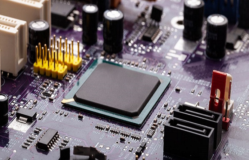
When is High Density Interconnect (HDI) PCB Required Instead of Conventional PCBs?
Conventional printed circuit boards serve as the backbone of basic electronic design, but as device complexity, miniaturization, and performance demands rise, high density interconnect (HDI) PCBs become a necessary upgrade. HDI technology leverages Sequential Lamination, microvias, and fine-pitch routing to solve the limitations of traditional boards, with compliance to IPC standards (IPC-2226, IPC-6012) ensuring reliability and manufacturability. Below is a structured breakdown of the core scenarios where HDI PCBs are the only viable solution, paired with technical specifics, industry benchmarks, and practical comparisons to guide design, procurement, and fabrication decisions.
Learn more about: How to Design HDI Microvia PCB
Extreme Miniaturization & Space Constraints
Miniaturization is the primary driver for HDI adoption, as consumer and industrial electronics demand more functionality in smaller form factors—an objective conventional PCBs cannot achieve due to their larger via sizes and lower routing density. HDI PCBs deliver 2–3x higher circuit density in the same physical area, making them indispensable for compact device design.
Core Technical Enablers for Miniaturization
- Laser-drilled microvias: With diameters as small as 75μm (0.003″) and aspect ratios of 1:1 or lower (per IPC-2226), microvias eliminate the space waste of conventional mechanical through-holes (minimum 0.3mm diameter).
- Sequential Lamination: Layer-by-layer build-up of dielectric and copper layers creates thin, compact stackups—an 8-layer conventional board can be replaced with a 6-layer HDI board with no loss in functionality.
- Fine trace spacing: HDI supports trace/space dimensions as low as 2mil (50μm), compared to the 6mil+ minimum for mass-produced conventional PCBs, maximizing surface and inner-layer routing efficiency.
Industry Benchmarks & Practical Comparisons
The table below quantifies the space efficiency gap between HDI and conventional PCBs for miniaturized designs:
| Design Aspect | HDI PCBs | Conventional PCBs |
|---|---|---|
| Pins per square inch | 120–160+ | <80 |
| Minimum microvia diameter | 75μm | N/A (mechanical holes only) |
| Typical board thickness for 6-layer design | 0.8–1.0mm | 1.2–1.6mm |
Target Applications & User Solutions
HDI is non-negotiable for devices where physical size is a hard constraint: wearables (smartwatches, fitness trackers), implantable medical devices (pacemakers), portable consumer electronics (smartphones, true wireless earbuds), and compact industrial sensors. For procurement and design teams, this means eliminating the need for multiple conventional boards in a single device—one HDI board integrates all functionality, reducing assembly complexity and device weight by up to 40%.
High-speed/high-frequency signal needs
Signal Integrity is the cornerstone of high-speed/high-frequency design, and conventional PCBs introduce critical flaws (via stubs, parasitic capacitance, crosstalk) that degrade signal performance at frequencies above 2GHz or data rates above 10Gbps. HDI PCBs are engineered to minimize these issues, making them the standard for 5G, RF, AI, and data center applications.
How HDI Enhances Signal Integrity
- Elimination of via stubs: Blind/buried microvias terminate at inner layers, removing the stubbed conductors that cause signal reflection and attenuation in conventional through-hole vias.
- Shorter signal paths: Denser component placement and fine-pitch routing reduce trace length, lowering signal delay and loss—critical for high-frequency RF and 5G millimeter-wave designs.
- Controlled impedance precision: HDI’s thin dielectric layers (0.08–0.2mm) and uniform copper plating enable impedance tolerance of ±8–10% (per IPC-6012 Class 3), compared to ±15% for conventional PCBs, ensuring consistent signal transmission.
Material & Process Requirements for High-Frequency HDI
- Low-loss dielectric materials: HDI designs use laminates with a stable dielectric constant (Dk 3.0–3.8) and low dissipation factor (Df <0.01) to reduce signal attenuation at high frequencies, a stark contrast to the standard FR-4 used in conventional PCBs (Dk 4.2–4.5, Df >0.02).
- Direct Metallization: Replaces electroless copper plating for microvia metallization, reducing hole wall roughness and parasitic capacitance—key for high-speed differential pairs (e.g., DDR5, PCIe 5.0).
Practical Design & Procurement Considerations
For engineers designing high-speed systems, HDI resolves the common pain point of balancing speed and manufacturability: conventional PCBs require costly back-drilling to remove via stubs, while HDI’s microvia technology achieves stub-free routing natively. This reduces fabrication time by 20–30% and eliminates back-drilling-related defects (e.g., incomplete stub removal).
Dense BGA/complex component fanout
Fine-pitch ball grid array (BGA) components (pitch ≤0.65mm, and ultra-fine pitch ≤0.4mm) are ubiquitous in modern electronics, but conventional PCBs lack the routing density to fan out these components without layer count bloat. HDI PCBs use microvias and via-in-pad (VIP) technology to enable efficient BGA fanout, a capability that directly addresses the design pain point of routing congestion.
HDI Fanout Technologies for Fine-Pitch BGAs
- Via-in-Pad (VIP): Laser-drilled microvias placed directly in BGA solder pads (copper-filled and capped) eliminate the need for dog-bone routing, freeing up 50% of surface space for additional components or shorter traces.
- Stacked/staggered microvias: Stacked microvias connect outer BGA layers to inner circuit layers vertically, while staggered microvias offset connections for ultra-fine pitch BGAs (0.2–0.4mm)—both eliminate the horizontal routing space required for conventional through-hole vias.
- Channel/boulevard routing: HDI’s laser-drilled microvias create parallel routing channels between BGA lands, enabling 2–4x more routing paths than conventional PCBs, which can only fit one through-hole via per BGA land gap.
IPC Standards & Manufacturability Benchmarks
- IPC/JPCA-2315 mandates that microvias for BGA fanout have a minimum annular ring of 75μm to ensure plating reliability—HDI manufacturers achieve this with laser direct imaging (LDI) (alignment accuracy ±20μm), while conventional PCBs (mechanical drilling) struggle with annular ring consistency for fine-pitch BGAs.
- For mass production, HDI supports BGA fanout for 0.2mm pitch components, while conventional PCBs are limited to ≥0.8mm pitch for cost-effective manufacturing.
Cost & Layer Count Comparisons
A common design challenge is layer count reduction: a conventional PCB for a 0.4mm pitch BGA requires 10–12 layers for fanout, while an HDI PCB achieves the same fanout with 6–8 layers (Sequential Lamination), reducing material costs by 25–30% despite higher HDI fabrication per-layer costs.
High component density & multi-function integration
Modern electronics demand the integration of diverse components (ICs, passives, sensors, RF modules) on a single board, and conventional PCBs fail here due to low routing density and fixed layer stackups. HDI PCBs enable high component density through flexible stackup design and efficient use of inner/outer layers, solving the procurement and design pain point of multiple board assemblies (MBAs) in compact devices.
HDI Stackup Designs for Integration
- 1+N+1 HDI: The most common stackup (1 build-up layer on each side of a core) supports moderate component density, ideal for consumer electronics (tablets, mid-range smartphones).
- 2+N+2 HDI: Two build-up layers on each core side enable stacked/staggered microvias and ultra-dense routing, for high-performance devices (AI edge computing modules, 5G modems).
- Any-layer HDI: All layers are build-up layers with copper-filled stacked microvias, enabling interconnection between any two layers—used for the most complex designs (GPU motherboards, medical imaging equipment).
Key Advantages Over Conventional Multi-Layer PCBs
- Component placement flexibility: HDI supports double-sided component placement with fine-pitch SMT (01005 passives) and through-hole components on the same board, while conventional PCBs require separate boards for different component types.
- Passive integration: HDI enables embedded passives (resistors, capacitors) in dielectric layers, reducing surface-mount component count by up to 30% and eliminating solder joint failure points.
- Reduced assembly complexity: One HDI board replaces 2–3 conventional PCBs in multi-function devices, cutting assembly time by 40% and reducing the risk of inter-board connection failures (e.g., cable or connector issues).
Industry Density Metrics
HDI PCBs achieve a wiring density (inches of trace per square inch) of 200–400, compared to 50–100 for conventional multi-layer PCBs. This metric, a key industry benchmark, quantifies HDI’s ability to integrate more functionality in the same space—critical for procurement teams evaluating board efficiency.
Thermal management in compact designs
High component density and miniaturization create heat concentration in electronic devices, and conventional PCBs have poor thermal dissipation due to thick dielectric layers and sparse via placement. HDI PCBs address this pain point with optimized copper distribution and thermal via design, ensuring reliable operation in high-power, space-constrained systems.
HDI Thermal Management Technologies
- Dense thermal vias: Laser-drilled microvias (0.1–0.2mm diameter) placed in thermal pads of high-power components (CPUs, GPUs, power amplifiers) create a direct heat path to ground planes—HDI supports up to 100 thermal vias per square millimeter, compared to 10–20 for conventional PCBs.
- Thin dielectric layers: HDI’s 0.08–0.1mm dielectric layers (vs. 0.2–0.4mm for conventional PCBs) improve thermal conductivity between copper layers, reducing heat buildup in inner layers.
- Copper-filled vias: Conductive copper filling in microvias and thermal vias increases heat transfer efficiency by 60–70% compared to non-filled vias in conventional PCBs, a requirement for high-power devices (e.g., EV BMS modules, AI server GPUs).
Material & Design Best Practices
- High-thermal-conductivity laminates: HDI designs use FR-4 with high glass transition temperature (Tg ≥170°C) or metal-core laminates for extreme thermal loads, while conventional PCBs use standard Tg 130°C FR-4.
- Copper pour optimization: HDI’s fine-pitch routing allows for continuous copper pours on inner layers (ground/power planes) with minimal trace interruptions, maximizing heat spreading—conventional PCBs have fragmented copper pours due to large via sizes.
Performance Quantification
In compact high-power designs (e.g., a 10W wearable sensor), an HDI PCB reduces component junction temperature by 15–20°C compared to a conventional PCB of the same size, extending component lifespan by 2–3x (per the Arrhenius equation for electronic reliability).
Reliability for harsh environments
Conventional PCBs fail in harsh environments (extreme temperatures, vibration, humidity, mechanical stress) due to their large through-hole vias (high aspect ratios, weak plating) and rigid stackups. HDI PCBs, built to IPC-6012 Class 3 and automotive IATF 16949 standards, deliver superior reliability by design, solving the critical pain point of field failure in industrial, automotive, aerospace, and military applications.
HDI Design Features for Harsh Environment Reliability
- Low-aspect-ratio microvias: Microvias with aspect ratios ≤1:1 (per IPC-2226) have thicker, more uniform plating than conventional through-holes (aspect ratios ≥6:1), eliminating plating cracking from thermal cycling (–40°C to +125°C).
- Sequential Lamination: Layer-by-layer bonding creates a more rigid, uniform board with minimal delamination risk—HDI PCBs pass 1,000+ thermal cycles (IPC-60068-2-14) without failure, compared to 500 cycles for conventional PCBs.
- Sealed vias: Tented/plugged microvias prevent moisture and contaminant ingress, a requirement for IP67/IP68-rated devices—conventional through-holes are prone to water intrusion without additional sealing.
Vibration & Mechanical Stress Resistance
- HDI’s dense microvia placement and thin, rigid stackups reduce board flexure under vibration (20–2,000Hz), a common issue for conventional PCBs with large through-holes that create stress points.
- Stacked microvias distribute mechanical stress across multiple layers, eliminating the single-point failure risk of conventional through-hole vias in high-vibration environments (e.g., automotive ADAS, aerospace avionics).
Industry Reliability Standards & Testing
HDI PCBs for harsh environments must comply with:
- IPC-6012 Class 3: For high-reliability electronics (aerospace, military), mandating 100% electrical testing and microvia cross-sectional analysis.
- IATF 16949: For automotive applications, requiring zero-defect manufacturing and traceability for all HDI components (laminates, copper foil, plating chemicals).
- IPC-60068-2-6: Vibration testing, where HDI PCBs demonstrate no electrical failure after 20 hours of random vibration (10–2,000Hz, 10g rms), while conventional PCBs often experience via plating cracking at 5g rms.
HDI vs. Conventional PCB: A Final Comparative Framework
For quick reference, the table below summarizes the core scenarios, technical capabilities, and cost tradeoffs that define the choice between HDI and conventional PCBs—an essential tool for design engineers and procurement teams:
| Decision Criterion | HDI PCBs | Conventional PCBs |
|---|---|---|
| Primary Use Case | Miniaturization, high-speed, dense BGA, harsh environments, multi-function integration | Basic electronics, low density, low frequency, cost-sensitive designs |
| Key Standards | IPC-2226, IPC/JPCA-2315, IPC-6012 Class 2/3 | IPC-2221, IPC-6012 Class 1/2 |
| Core Process | Sequential Lamination, laser drilling, direct metallization | Standard lamination, mechanical drilling, electroless copper plating |
| Cost Premium (Mass Production) | 2–3x conventional PCBs | 1x (baseline cost) |
| Layer Count Efficiency | 20–40% fewer layers for equivalent functionality | Higher layer count for dense/routed designs |
| Reliability (Harsh Environments) | Exceeds 1,000 thermal cycles, IP67/IP68 compatible | ≤500 thermal cycles, limited environmental sealing |
Conclusion
High density interconnect (HDI) PCBs are not just a premium alternative to conventional PCBs—they are a necessary solution when electronic design demands miniaturization, high-speed Signal Integrity, dense component integration, efficient thermal management, or harsh-environment reliability. By leveraging Sequential Lamination, laser-drilled microvias, and compliance with IPC industry standards, HDI resolves the core pain points of conventional PCB design and manufacturing, delivering quantifiable improvements in performance, density, and reliability. For design engineers, procurement teams, and electronic enthusiasts, the key takeaway is clear: HDI PCBs are the standard for modern, high-performance electronics, while conventional PCBs remain viable only for basic, low-density, cost-sensitive applications. Understanding this distinction is critical to optimizing device design, reducing fabrication costs, and ensuring long-term product reliability.


