
DFM for HDI circuit boards enables consistent, high-yield production by standardizing via structures, trace geometries, material selection, and stackup design to align with real-world fabrication capabilities. Following strict manufacturing rules reduces assembly risks, shortens lead times, and ensures compliance with IPC‑6012 and IPC‑2226 requirements for high density interconnect designs.
Learn more about :How to Design HDI Microvia PCB
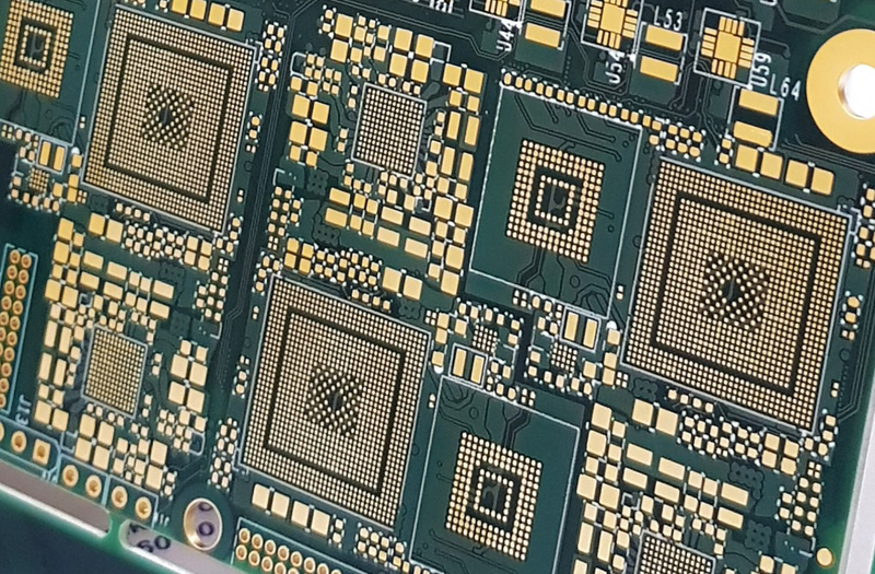
Technical Points
1. Via Technology & Placement
Prefer Staggered Vias
- Staggered via layouts reduce mechanical stress and plating voids compared to stacked structures
- Maintain horizontal spacing between staggered vias at ≥ 0.20 mm (8 mil)
- Reduces thermal fatigue failure by approximately 40% under cyclic loading
- Complies with IPC‑4761 Type III and IV design rules
Microvia Size Specifications
- Recommended microvia diameter range: 0.10 mm to 0.15 mm (4 to 6 mil)
- Aspect ratio limited to ≤ 0.75:1 for consistent copper plating
- Minimum drill depth accuracy controlled within ± 0.025 mm (1 mil)
- Laser drilling preferred for vias smaller than 0.15 mm (6 mil)
Blind / Buried Vias & Via‑in‑Pad
- Blind vias connect outer layers to one inner layer without full penetration
- Buried vias exist only between internal layers and improve routing density
- Via‑in‑Pad (VIP) requires full copper filling and planarization ≤ 0.005 mm (0.2 mil)
- VIP structures support 0.4 mm and 0.5 mm pitch BGA components
Learn more about : What is Via-in-Pad? HDI PCB Benefits & Manufacturing Process
2. Trace and Spacing Rules
Line / Space Width Standards
- Minimum production‑stable line/space: 0.0635 mm / 0.0635 mm (2.5 / 2.5 mil)
- High‑volume designs recommended: 0.100 mm / 0.100 mm (4 / 4 mil)
- Impedance control requires dielectric tolerance within ± 10%
- Trace width deviation maintained within ± 0.005 mm (0.2 mil)
Avoid Trace Necking
- Minimum trace width reduction limited to ≤ 10% of original width
- Necking below 0.050 mm (2 mil) causes current‑density overheating
- Reduces reliability by increasing open‑circuit failure risk
- Sustains current‑carrying capacity per IPC‑2221 current‑density tables
3W Rule Implementation
- Trace center‑to‑center spacing ≥ 3× the trace width
- Reduces crosstalk by 20–25 dB in high‑speed differential pairs
- Mandatory for 5G, SerDes, and RF signal paths above 1 Gbps
- Maintains signal integrity and impedance consistency
3. Material and Stackup Design
Early Fabrication Involvement
- Preliminary stackup review before 50% design completion
- Validate dielectric thickness, copper weight, and material availability
- Confirm sequential lamination cycle limits (1 to 4 cycles)
- Prevents material incompatibility and 2–3 week lead‑time delays
Material Selection Parameters
- Tg value ≥ 135°C for standard designs; ≥ 170°C for automotive/industrial
- CTE X‑Y ≤ 16 ppm/°C for stable via and pad performance
- Moisture absorption limited to ≤ 0.15% before reflow
- Compatible with lead‑free assembly at 260°C peak temperature
4. Surface Finish and Testing
Surface Finish Options
- ENIG: Ni 3–6 μm, Au 0.05–0.15 μm for general HDI applications
- ENEPIG: enhanced reliability for fine‑pitch BGAs and wire bonding
- Immersion silver for cost‑sensitive high‑volume designs
- All finishes meet IPC‑4552 and IPC‑4556 specifications
Quality and Reliability Testing
- Microsection analysis for via fill and plating uniformity
- Thermal cycling: –40°C to 125°C, 500 to 1000 cycles
- Solderability testing per IPC‑J‑STD‑004
- Impedance verification with TDR test coupons
5. Fabrication Guidelines
Annular Ring Requirements
- Outer layer annular ring: ≥ 0.050 mm (2 mil)
- Inner layer annular ring: ≥ 0.040 mm (1.6 mil)
- Prevents breakout during drilling and lamination
- Complies with IPC‑6012 Class 2 and Class 3 requirements
Board Edge Clearance
- Minimum distance from via/trace to board edge: 0.3 mm (12 mil)
- Route keep‑out zone ≥ 0.5 mm (20 mil) for high‑speed signals
- Reduces edge‑chipping and routing damage during depaneling
- Supports V‑cut and laser depaneling processes
Data Package Standards
- Complete Gerber X2 layer set including signal, power, ground, mask, silk
- Accurate NC drill and rout files with via classification
- Stackup diagram, impedance table, and IPC class specification
- Netlist and DFM report for pre‑production validation
6. Key Comparison Tables
Stacked Vias vs. Staggered Vias
| Aspect | Stacked Vias | Staggered Vias |
|---|---|---|
| Density | Higher | Moderate |
| Reliability | Lower | Higher |
| Failure Risk | Higher thermal fatigue | Lower stress concentration |
| Recommended Use | Ultra-compact consumer HDI | Industrial/automotive HDI |
ENIG vs. ENEPIG Surface Finishes
| Aspect | ENIG | ENEPIG |
|---|---|---|
| Solderability | Good | Excellent |
| Corrosion Resistance | High | Very High |
| Fine-pitch BGA Suit | Moderate | Ideal |
| Cost | Standard | 1.4–1.6× higher |
Factory Case Study
12‑Layer HDI Board for 5G Small Cell
Project Specifications
- Layer structure: 2+8+2 high density interconnect stackup
- Materials: high‑Tg FR‑4 (Tg 175°C, CTE 14 ppm/°C)
- Target line/space: 0.0635 mm / 0.0635 mm (2.5/2.5 mil)
- Microvia size: 0.125 mm (5 mil), aspect ratio 0.7:1
- Impedance: 50Ω single‑ended, 100Ω differential
Issues Encountered
- Stacked vias caused 23% microvia cracking during thermal cycling
- Trace necking below 0.050 mm (2 mil) led to 14% open circuits
- Annular rings of 0.03 mm (1.2 mil) resulted in drill breakout
- Missing DFM review delayed production by 18 days
Improvements Implemented
- Changed from stacked to staggered via layout
- Enforced minimum trace width ≥ 0.0635 mm (2.5 mil)
- Increased annular rings to ≥ 0.050 mm (2 mil)
- Conducted pre‑layout DFM review with fabrication team
Results
- Yield improved from 71% to 94%
- Thermal cycle failure rate reduced from 23% to 2%
- Production lead time shortened by 14 days
- No BGA assembly or signal‑integrity failures
Common Design Errors
- Using stacked vias without aspect‑ratio control leads to plating voids and reliability risks.
- Trace necking below 0.050 mm (2 mil) causes current‑density hotspots and opens.
- Insufficient annular rings below 0.040 mm (1.6 mil) result in drill breakout and electrical opens.
- Missing via‑fill specification for via‑in‑pad causes solder wicking and BGA defects.
- Incomplete Gerber data without stackup or impedance notes leads to misfabrication.
- Violating the 3W rule increases crosstalk and fails high‑speed compliance tests.
FAQ
1. What is the difference between PCB and PCA in HDI manufacturing?
A PCB is the bare printed circuit board, while a PCA is a printed circuit assembly with components soldered. DFM errors in HDI PCB design—such as inadequate annular rings or poor via structures—directly cause assembly failures in the PCA.
2. Why is staggered via placement preferred over stacked vias in HDI?
Staggered vias reduce mechanical stress and plating voids, improve thermal‑cycle reliability, and lower failure rates by approximately 40% compared to stacked vias, making them preferred for industrial and automotive high density interconnect boards.
3. What is the minimum stable line/space for mass‑produced HDI circuit boards?
The minimum stable line/space for mass production is 0.0635 mm / 0.0635 mm (2.5/2.5 mil). Values below this significantly reduce yield and increase manufacturing cost and risk.
4. What is the purpose of the 3W rule in HDI PCB design?
The 3W rule requires trace spacing equal to three times the trace width, which reduces crosstalk, preserves signal integrity, and maintains controlled impedance for high‑speed circuits in high density interconnect PCBs.
If you need HDI PCB manufacturing or design support, our engineering team provides free DFM analysis and quotation.


![Understanding PCB Costs & Pricing [Your Complete Guide]](https://hdicircuitboard.com/wp-content/uploads/elementor/thumbs/Understanding-PCB-Costs-Pricing-Your-Complete-Guide-qzzhe6mcaxuolkux3xalfktgavumi9y1aqfbs9bpv4.webp "Understanding PCB Costs & Pricing [Your Complete Guide]")


