
Flexible PCB impedance control requires precise management of dielectric materials, copper parameters, reference planes, and bend characteristics to maintain signal integrity in dynamic applications. This factory-engineered guide provides exact specifications, material properties, design formulas, and quality control methods for single-ended, differential, and coplanar impedance structures in flexible printed circuit boards and rigid-flex PCB assemblies.
Learn more about: Flexible PCB Design Guidelines
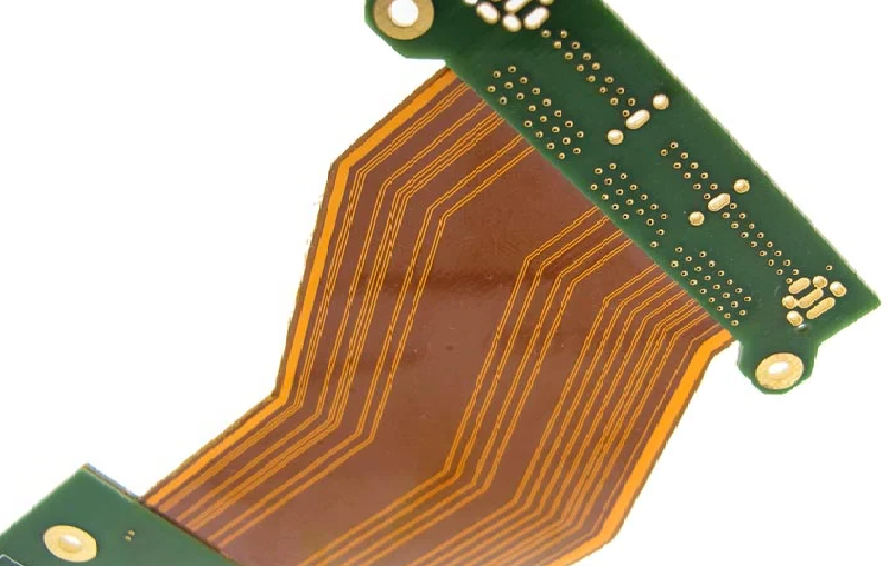
Key Factors in Flexible PCB Impedance Control
Dielectric Material Properties
- Polyimide (PI) Base Materials
- Standard Dk values: 3.1-3.5 (1MHz)
- High-temperature variants: 3.3-3.7 Dk
- Thickness options: 12.5μm, 25μm, 50μm, 75μm
- Tolerance: ±5% (IPC-4101E)
- Loss tangent: 0.002-0.004 @10GHz
- Adhesive Layer Parameters
- Acrylic adhesive: Dk 3.2-3.6, thickness 15-25μm
- Epoxy adhesive: Dk 3.5-4.0, thickness 10-20μm
- Bonding film: Dk 3.0-3.4, thickness 12-18μm
- No-adhesive systems: Dk 3.1-3.3, zero bond layer
- Coverlay/Coating Materials
- Coverlay thickness: 12.5μm, 25μm, 50μm
- Solder mask Dk: 3.3-3.7, thickness 10-15μm
- Bonding adhesive: 10-15μm thickness
- Total dielectric stack: 0.05-0.20mm
Copper Characteristics
- Copper Thickness Options
- Ultra-thin: 5μm (1/7oz) for dynamic flexing
- Standard: 12μm (1/3oz), 18μm (1/2oz)
- Heavy: 35μm (1oz) for power circuits
- Tolerance: ±1μm (Class 3), ±1.5μm (Class 2)
- Copper Type Selection
- Rolled Annealed (RA): 0.2% elongation, ideal for dynamic bending
- Electrodeposited (ED): 0.1% elongation, static applications
- Surface roughness: <0.5μm (Ra) for high-frequency
- IPC-4562A specification compliance
Cross Hatched Planes
- Mesh Density Parameters
- Standard pattern: 0.5mm × 0.5mm grid
- Line width: 0.15-0.25mm
- Open area: 50-70%
- Impedance shift: +3-8% vs solid plane
- Design Rules
- Minimum web width: 0.15mm
- Corner radius: 0.2mm minimum
- Connection points: every 5mm maximum
- Symmetric pattern across layer
- Electrical Performance
- Shielding effectiveness: 20-30dB @1GHz
- Current capacity: 60-70% of solid plane
- Bend flexibility: 3× improved vs solid plane
- Impedance stability: ±2% across bend area
Common Impedance Types
Single Ended Microstrip
- Standard Configurations
- Target impedance: 50Ω ±5% (IPC-2223)
- Dielectric thickness: 0.05-0.15mm
- Copper thickness: 12-18μm
- Line width: 0.18-0.35mm
- Calculation Formula
- Z0 = (87/√(Dk+1.41)) × ln(5.98H/(0.8W+T))
- H = dielectric thickness (mm)
- W = trace width (mm)
- T = copper thickness (mm)
- Manufacturing Tolerances
- Width tolerance: ±0.02mm
- Thickness tolerance: ±0.005mm
- Impedance tolerance: ±5% (Class 2), ±3% (Class 3)
Differential Pair Microstrip
- Standard Parameters
- Impedance: 90Ω, 100Ω ±8%
- Line width: 0.12-0.25mm
- Spacing: 0.15-0.30mm
- Dielectric: 0.075-0.15mm thickness
- Design Requirements
- Length matching: ±0.1mm maximum difference
- Parallelism: maintained over entire length
- Symmetric environment: identical spacing on both sides
- Bend radius: >10× thickness for differential pairs
- Coupling Control
- Edge-to-edge spacing: 1.5-2.5× line width
- Impedance reduction: 10-15% with tight coupling
- Skew control: <0.5ps/cm propagation difference
Coplanar Lines
- Structure Parameters
- Signal line: 0.10-0.20mm width
- Ground gap: 0.15-0.25mm
- Ground width: 0.20-0.35mm
- Impedance: 50Ω ±6%
- Advantages
- Reduced crosstalk: 40% improvement
- Bend stability: ±2% impedance variation
- Space efficiency: 30% smaller footprint
- Easier manufacturing: single-layer processing
Learn more about: Flexible PCB Material: Adhesive vs Adhesiveless, RA vs ED Copper
Design Best Practices
Reference Plane Management
- Continuity Requirements
- No gaps within 3× trace width
- Minimum plane extension: 2× trace width
- Via stitching: 0.5mm spacing along edges
- Cross-hatching in dynamic bend areas
- Layer Stack-up Optimization
- 2-layer: Signal-GND
- 4-layer: Signal-GND-PWR-Signal
- 6-layer: Signal-GND-Signal-PWR-GND-Signal
- Dielectric thickness: 0.075mm standard
Bend Radius Considerations
- Static Bending
- Minimum radius: 6× total thickness
- Impedance shift: <3%
- Copper stress: <0.1% elongation
- Dynamic Bending
- Minimum radius: 10× total thickness
- Maximum cycles: 10,000-100,000
- Impedance stability: ±5% over lifetime
- Copper type: RA copper mandatory
Simulation and Verification
- Pre-layout Simulation
- 2D field solver: Polar Instruments, Si9000
- Parameters: Dk, thickness, copper profile
- Temperature range: -40°C to +125°C
- Frequency: DC to 20GHz
- Post-fabrication Testing
- TDR measurement: IPC-TM-650 2.5.5.7
- Sample size: 5% of production panels
- Test points: every 50mm of impedance trace
- Acceptance criteria: ±5% of target
Critical Parameter Comparisons
Solid vs. Cross-Hatched Planes
| Parameter | Solid Plane | Cross-Hatched Plane |
|---|---|---|
| Impedance Accuracy | ±2% | ±5% |
| Bend Flexibility | Low | High (3× better) |
| Shielding Effectiveness | 35-45dB | 20-30dB |
| Current Capacity | 100% | 60-70% |
| Weight | Standard | 30% lighter |
| Material Stress | High | Low |
Single-ended vs. Differential Impedance
| Feature | Single-ended (50Ω) | Differential (100Ω) |
|---|---|---|
| Trace Width | 0.20-0.35mm | 0.12-0.25mm |
| Spacing Requirement | N/A | 0.15-0.30mm |
| Noise Immunity | Standard | High (20dB better) |
| Bend Sensitivity | Medium | High |
| Space Requirement | Low | High (40% more) |
| Common Applications | USB 2.0, RF | USB 3.0, HDMI, LVDS |
Learn more about: Flexible PCB Layer Stackup: Complete Design Guide
Core Technical Parameters
Impedance Table
- 50Ω Single Ended (PI Dk=3.3)
- H=0.075mm, T=18μm: W=0.28mm
- H=0.10mm, T=18μm: W=0.36mm
- H=0.125mm, T=18μm: W=0.44mm
- 100Ω Differential (PI Dk=3.3)
- H=0.075mm, T=18μm: W=0.18mm, S=0.22mm
- H=0.10mm, T=18μm: W=0.22mm, S=0.28mm
- H=0.125mm, T=18μm: W=0.26mm, S=0.34mm
Manufacturing Specifications
- Line Width/Spacing
- Minimum: 0.10mm/0.10mm (Class 3)
- Standard: 0.12mm/0.12mm (Class 2)
- Tolerance: ±0.02mm (etch factor 1.5-2.0)
- Layer Count Guidelines
- 2-layer: up to 5GHz bandwidth
- 4-layer: up to 15GHz bandwidth
- 6-layer: up to 20GHz+ bandwidth
- Quality Control Metrics
- Impedance test coverage: 100% critical signals
- TDR resolution: 50μm
- Measurement bandwidth: DC to 10GHz
- Acceptance: IPC-6013 Class 2/3 standards
Case Study
Project Specifications
- Product: Automotive camera system flexible PCB
- Configuration: 4-layer rigid-flex, 0.12mm flex thickness
- Requirements: 50Ω single-ended, 100Ω differential ±5%
- Environment: -40°C to +105°C, 5,000 flex cycles
Initial Design Issues
- Problem 1: 12% impedance deviation in bend areas
- Problem 2: Differential pair skew >2ps/cm
- Problem 3: Signal degradation after 1,500 cycles
Engineering Solutions
- Changed from solid to cross-hatched reference planes (0.5mm grid)
- Optimized differential pair geometry: W=0.18mm, S=0.22mm
- Increased bend radius from 0.75mm to 1.25mm (10× thickness)
- Implemented teardrop transitions at rigid-flex boundaries
- Added via stitching at 0.5mm intervals along plane edges
Final Results
- Impedance Accuracy: 50.2Ω ±2.1%, 99.6Ω ±3.2%
- Cycle Life: 7,500+ cycles (50% improvement)
- Production Yield: 96.2% (from 78.5%)
- Signal Integrity: 30% reduction in insertion loss
Common Design Errors
- Incorrect Dielectric Selection: 43% of impedance failures (wrong Dk value)
- Insufficient Bend Radius: 38% of flex fatigue issues (under 10× thickness)
- Reference Plane Discontinuities: 35% of impedance deviations (gaps near traces)
- Differential Pair Asymmetry: 32% of skew issues (length mismatch >0.1mm)
- Wrong Copper Type: 29% of dynamic failures (ED copper in flex zones)
- Inadequate Simulation: 27% of prototype failures (no thermal analysis)
- Poor Transition Design: 24% of rigid-flex failures (abrupt thickness changes)
- Ignoring Coverlay Effects: 22% of impedance shifts (unaccounted 12.5μm layer)
Frequently Asked Questions
Q: What impedance tolerance is standard for flexible PCBs?
A: IPC-2223 specifies ±5% for Class 2 general applications and ±3% for Class 3 high-reliability products. Flexible circuits typically allow ±5% due to material and bending variations, with critical high-speed circuits requiring ±3% precision.
Q: How does bending affect flexible PCB impedance?
A: Static bending (<6× thickness) causes <3% impedance shift. Dynamic bending requires radius >10× thickness to maintain ±5% stability. Cross-hatched planes reduce bending-related impedance variation by 40-50% compared to solid planes.
Q: What’s the difference between microstrip and coplanar structures?
A: Microstrip uses a solid reference plane below the signal trace (50Ω standard). Coplanar structures have ground conductors on the same layer (±6% tolerance). Coplanar designs offer 30% better space efficiency and 40% improved bend stability.
Q: How to specify impedance requirements to manufacturers?
A: Provide exact stack-up (dielectric Dk/thickness), copper weight, target impedance with tolerance, trace geometry, and reference plane type. Include IPC class (2/3), bend requirements, and test methodology (IPC-TM-650 2.5.5.7).
If you need professional flexible circuit board design support or quotation, our team provides free DFM check and fast turnaround.


