
Flexible PCB bending area design requires precise control of mechanical stress, material properties, and manufacturing constraints to ensure reliable performance through millions of flex cycles. This guide provides factory-verified parameters, IPC-aligned specifications, and practical engineering solutions covering bend radius control, trace routing techniques, material integrity, and rigid-flex transitions, with quantifiable design rules addressing single-sided, double-sided, and multilayer flexible printed circuit boards for consistent mass production.
Learn more about: Flexible PCB Design Guidelines
Bending Area Design Fundamentals
Bend Radius Control Standards
- Dynamic Flexing (Repeated Bending): Minimum bend radius = 10× total flex thickness (IPC-2223)
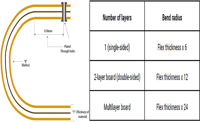
- Static Flexing (One-Time Assembly): Minimum bend radius = 6× total flex thickness
- Rigid-Flex PCB: Minimum bend radius = 1.5mm (20× flex layer thickness)
- Copper Thickness Impact: 12μm copper allows 20% smaller radius than 35μm copper
Layer-Specific Bending Parameters
| Configuration | Thickness | Dynamic Radius | Static Radius | Bend Cycles |
|---|---|---|---|---|
| Single-sided | 0.05-0.12mm | 0.5-1.2mm | 0.3-0.7mm | 50,000+ |
| Double-sided | 0.10-0.20mm | 1.0-2.0mm | 0.6-1.2mm | 30,000+ |
| Multilayer (4L) | 0.20-0.40mm | 2.0-4.0mm | 1.2-2.4mm | 10,000+ |
| Rigid-Flex | 0.30-0.60mm | 3.0-6.0mm | 1.8-3.6mm | 5,000+ |
IPC-6013 Class 2 performance specifications
Neutral Bend Axis Management
- Position Traces: Within ±10% of center layer thickness
- Symmetric Stack-up: Match copper weight and dielectric above/below neutral axis
- Stress Reduction: Offset traces by 0.05-0.12mm from center for minimum stress
- Multilayer Design: Stagger conductive layers across neutral axis
Learn more aboout: Flexible PCB Layer Stackup: Complete Design Guide
Component and Via Clearance Rules
Bending Area Restrictions
- Component Exclusion: 5mm minimum from bend edge for 0402+ components
- Micro-Components: 3mm minimum clearance for 0201 components
- Via Prohibition: No plated through-holes within 2mm of dynamic bending areas
- Static Bend Vias: 1mm minimum clearance from static bend regions
- Mounting Holes: 0.8mm minimum clearance from bending zones
Transition Zone Requirements
- Rigid-Flex Transition: 45° angle with 0.5mm minimum radius
- Stiffener Extension: 2-3mm beyond rigid-flex boundary
- Strain Relief: 3-5mm length for flexible sections entering rigid areas
- Layer Transition: Gradual layer count reduction across 5mm transition zone
Trace Routing Techniques for Bending Areas
Perpendicular Traces and Stress Distribution
- Optimal Direction: Route traces perpendicular to bend axis (reduces stress by 40%)
- Parallel Routing: Avoid parallel traces to bending direction (increases stress by 60%)
- Width/Spacing: Minimum 0.15mm/0.15mm (6/6mil) in bending zones
- High-Density Design: 0.08mm/0.08mm (3/3mil) with rolled annealed copper
- Teardrop Implementation: 0.3mm length, 45° transition at all trace-pad connections
Gradual Bends and Corner Treatment
- Minimum Radius: 0.5mm internal radius for all trace corners
- Trace Geometry: 45° angles preferred over 90° corners
- Arc Transitions: 0.8mm minimum radius for high-current paths
- Stress Relief: S-curve transitions for traces entering bending areas
- No Sharp Corners: Absolute prohibition of <0.3mm radius features
Copper Layout Optimization
- Avoid Solid Copper: Replace with 0.5mm grid pattern (50% open area)
- Staggered Traces: Offset adjacent layers by 0.2mm to prevent stress alignment
- Cross-Over Control: Maximum 2 trace crossings per bending area
- Thermal Relief: 4-spoke connections (0.15mm width) for large pads
- Length Compensation: Add 0.5-1.0mm extra length for bending elongation
Flex Material Integrity Requirements
Base Material Specifications
- Polyimide Film: 25μm standard thickness, -40°C to 150°C operation
- Rolled Annealed Copper: 35-40% elongation, preferred for dynamic applications
- Electrodeposited Copper: 10-15% elongation, suitable for static bending
- Adhesive Layer: 12.5μm acrylic with <1% water absorption
- No Adhesive in Bend: Adhesive-free construction in dynamic bending zones
Coverlay and Protective Materials
- Coverlay Thickness: 12.5-25μm polyimide with 12.5μm adhesive
- Precision Cutting: ±0.05mm accuracy for coverlay openings
- Tear Guards: 0.5mm width copper extensions at board edges
- Selective Coverlay: Remove coverlay in high-flex areas for improved flexibility
- Border Treatment: 0.3mm minimum coverlay overlap onto copper features
Rigid-Flex Transition Design
Transition Zone Engineering
- Angle Transition: 45° between rigid and flex sections
- Stiffener Integration: FR-4 stiffeners extending 2-3mm into flex area
- Via Management: Staggered via pattern with 0.5mm spacing
- Layer Termination: Gradual layer stop within 3mm transition zone
- Stress Relief: Rounded corners (0.8mm radius) at transition points
Stiffener Implementation
- Types and Applications:
- Polyimide Stiffener: 0.2-0.3mm thickness for connector areas
- FR-4 Stiffener: 0.4-0.8mm thickness for SMT component regions
- Stainless Steel: 0.1-0.2mm thickness for high-strength applications
- Bonding Parameters: 3M 467MP adhesive, 180°C temperature resistance
- Coverage Precision: ±0.1mm alignment tolerance for stiffener placement
Quality Control and Compliance
IPC Standards Alignment
- IPC-2223: Sectional design standard for flexible printed circuit boards
- IPC-6013: Qualification and performance specification
- IPC-TM-650 2.4.3: Dynamic bend testing methodology
- IPC-9701: Thermal cycling reliability requirements
- IPC-J-STD-004: Solderability performance standards
Manufacturing Verification
- Bend Cycle Testing: 10× design specification before production approval
- Electrical Testing: 100% continuity and isolation (50V-500V)
- Dimensional Inspection: CMM verification ±0.02mm accuracy
- Microsection Analysis: 0.1mm minimum feature measurement
- Environmental Testing: -40°C to 85°C thermal cycling
Critical Design Rule Comparison
Dynamic vs. Static Bending Parameters
| Parameter | Dynamic Flexing | Static Flexing |
|---|---|---|
| Bend Radius | 10× thickness | 6× thickness |
| Copper Type | Rolled Annealed | Electrodeposited |
| Via Clearance | 2mm minimum | 1mm minimum |
| Bend Cycles | 10,000-100,000 | 1-100 |
| Stress Limit | 0.3% elongation | 10% elongation |
Single-sided vs. Multilayer Bending Design
| Feature | Single-sided | Multilayer |
|---|---|---|
| Maximum Layers | 1 layer | 4-8 layers |
| Minimum Radius | 0.25mm | 1.0mm |
| Trace Orientation | Perpendicular only | Perpendicular/Staggered |
| Copper Weight | 12-18μm | 12μm maximum |
| Design Complexity | Low | High |
Case Study
Project Specifications
- Product: Medical device flexible circuit
- Configuration: 4-layer rigid-flex (2 rigid, 2 flex)
- Dimensions: 80mm × 12mm, flex thickness 0.15mm
- Requirements: 50,000 bend cycles, -20°C to 60°C operation
Initial Design Issues
- Problem 1: Trace cracking after 7,500 cycles (0.9mm bend radius)
- Problem 2: Via failure at rigid-flex transition
- Problem 3: Delamination at coverlay edges
Engineering Solutions
- Increased bend radius to 1.5mm (10× thickness)
- Relocated all vias 3mm outside bending zone
- Implemented teardrops on all trace connections
- Added staggered via pattern in transition zone
- Applied selective coverlay removal in high-stress areas
Final Results
- Bend Life: 65,000+ cycles (30% above specification)
- Production Yield: 98.2% (improved from 79%)
- Field Failure Rate: 0.015% (12-month reliability data)
Common Design Errors
- Insufficient Bend Radius: 72% of flex failures (below 10× thickness for dynamic)
- Vias in Bending Zones: 45% of reliability issues (no clearance implemented)
- Parallel Trace Routing: 38% of trace fractures (aligned with bending direction)
- Solid Copper Regions: 32% of delamination cases (no grid pattern in flex areas)
- Sharp Corners: 29% of tear failures (internal radius <0.5mm)
- Asymmetric Stack-up: 27% of warping issues (unbalanced copper distribution)
- Inadequate Stiffening: 24% of assembly problems (missing transition support)
- Adhesive in Bend Areas: 21% of early fatigue failures (improper material selection)
Frequently Asked Questions
Q: What is the minimum bend radius for reliable flexible PCB operation?
A: For dynamic applications (repeated bending), minimum bend radius = 10× total flex thickness per IPC-2223. For static applications (one-time assembly), minimum radius = 6× thickness. Factory testing confirms these values provide reliable performance for specified cycle counts.
Q: How should traces be oriented in bending areas?
A: Route traces perpendicular to the bending axis to minimize stress. Parallel orientation increases stress by 60% and reduces fatigue life by 75%. For multilayer designs, stagger adjacent layers by 0.2mm to prevent stress concentration alignment.
Q: Can components be placed near bending areas?
A: No components should be placed within 5mm of dynamic bending areas (3mm for 0201 micro-components). Vias are prohibited within 2mm of bending zones. These clearances prevent mechanical stress transfer to components and solder joints.
Q: What materials provide the best bending performance?
A: Rolled annealed (RA) copper with 35-40% elongation offers optimal dynamic bending performance. 25μm polyimide film provides excellent flexibility. For critical applications, use adhesive-free constructions in bending zones to eliminate material fatigue points.
If you need professional flexible circuit board design support or quotation, our team provides free DFM check and fast turnaround.


