
Rigid-flex PCB represents a hybrid circuit solution that integrates rigid dielectric substrates and flexible polyimide layers into a single unified laminated structure. Combining stable rigid zones for component soldering and mechanical mounting with bendable flexible sections for dynamic assembly and three-dimensional packaging, this board type eliminates external connectors, reduces overall assembly complexity, and enhances long-term operational stability. Produced in full compliance with IPC-2221 and IPC-6013 industrial standards, rigid-flex PCB addresses miniaturization demands while maintaining reliable signal performance, mechanical durability, and thermal adaptability across consumer, medical, aerospace, and automotive industries.
Learn more about: Rigid-Flex PCB Manufacturing Process Step by Step
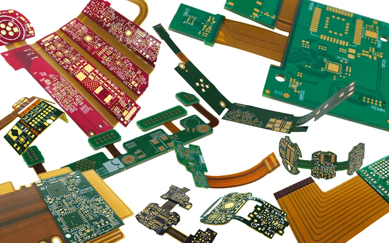
What is Rigid Flex PCB
Integrated Hybrid Circuit Construction
Rigid-flex PCB merges rigid FR-4 core materials and thin polyimide flexible films through high-pressure thermal lamination, forming an integrated circuit without secondary bonding or assembly separation. Rigid segments deliver structural rigidity for surface-mount components, heavy connectors, and heat-generating chips, while lightweight polyimide flexible areas support repeated bending, folding, and spatial deflection. Unlike discrete rigid boards paired with independent flex cables, the monolithic design cuts redundant connection points, lowers contact failure risks, and streamlines overall product structural layout.
Industry Standard Compliance Framework
Universal manufacturing and design regulations govern rigid-flex PCB production to ensure cross-industry consistency and reliability. IPC-6013 establishes performance grading criteria for flexible and rigid-flex circuits, covering bending durability, insulation resistance, and lamination integrity. IPC-2221 defines critical design rules including trace width, dielectric thickness, and impedance control parameters. High-reliability application scenarios adopt IPC Class 3 specifications, requiring full electrical testing, thermal cycling validation, and mechanical bending endurance testing before mass shipment.
Learn more about: What is a Rigid-Flex PCB? Design & Manufacturing Best Practices
Key Features and Benefits
| Parameter | Rigid-Flex PCB | Flex PCB With Stiffeners |
|---|---|---|
| Integrated Structure | Monolithic lamination | Secondary bonding assembly |
| Cyclic Bending Life | 10,000 – 100,000 cycles | 1,000 – 5,000 cycles |
| Boundary Stress Risk | Low | High |
| High-Speed Signal Stability | Controlled ±5% impedance | Obvious impedance drift |
| Long-Term Aging Resistance | Industrial grade durability | Limited adhesive service life |
Space & Weight Saving
Integrated rigid-flex architecture removes bulky wiring harnesses, intermediate connection terminals, and auxiliary fixing parts. Verified manufacturing data proves this design reduces internal device space occupancy by 30% to 60% and cuts overall product weight by 40% to 70%. Shortened internal signal routing optimizes compact enclosure design, making rigid-flex PCB ideal for ultra-thin wearables, foldable devices, and portable precision electronics with limited internal installation space.
Improved Reliability
Fewer mechanical connection interfaces greatly reduce failure causes such as connector loosening, metal oxidation, and vibration-induced signal interruption. Integrated lamination technology enhances overall structural cohesion, delivering 10G to 20G anti-vibration resistance for harsh working environments. Precision impedance control maintains signal transmission deviation within ±5% tolerance, while continuous ground layer layout suppresses high-frequency crosstalk and electromagnetic interference for stable long-duration operation.
Design Freedom
Customizable mixed layout of rigid and flexible zones supports non-planar installation, curved routing, and multi-angle folding configurations. Design engineers can partition functional areas based on enclosure contours and mechanical movement requirements, breaking the limitations of traditional planar circuit boards. Advanced high density interconnect technology adopts laser-drilled microvias with a minimum aperture of 0.1mm, enabling dense layer-to-layer conduction and meeting high-complexity miniaturized circuit wiring demands.
Optimized Electrical Performance
Matched dielectric materials maintain stable dielectric constant and low loss tangent in high-frequency working conditions. Integrated conductive pathways avoid signal attenuation and delay caused by multi-segment connection transitions. Balanced copper foil thickness configuration in flexible and rigid areas ensures consistent current carrying capacity and electrical stability, withstanding long-term temperature fluctuations ranging from -40°C to 125°C without performance degradation.
Usage Examples
Consumer Electronics
Consumer electronic hardware remains the largest application market for mass-produced rigid-flex PCB. Foldable smartphones, smart wearables, miniature camera modules, and handheld Bluetooth devices widely adopt 4-layer to 12-layer rigid-flex structures. Flexible hinge modules use high-elongation rolled copper foil to sustain 50,000+ cyclic bends, while surface anti-oxidation plating processes extend service life for daily frequent bending and extrusion scenarios.
Medical Devices
Portable diagnostic instruments, minimally invasive surgical tools, and wearable health monitoring equipment adopt medical-grade rigid-flex PCB materials. Biocompatible polyimide substrates and high-purity surface finishes meet medical environmental adaptability requirements, resisting high-temperature disinfection and humid working conditions. Ultra-thin integrated stacking designs adapt to the narrow internal space of precision medical devices, balancing structural flexibility and electrical safety.
Aerospace & Defense
Aerospace and defense electronic equipment requires ultra-high reliability rigid-flex PCB solutions. Multi-layer high-Tg laminated structures, radiation-resistant coatings, and low thermal expansion coefficient materials adapt to extreme temperature differences and complex space environments. Strict mechanical shock and vibration testing ensures stable operation for avionics control units, satellite communication modules, and military rugged display systems under severe working conditions.
Automotive
Modern automotive electronic systems including ADAS sensing modules, in-vehicle infotainment, and new energy battery management units extensively apply automotive-qualified rigid-flex PCB. Complying with AEC-Q100 Grade 1 standards, these circuits withstand extreme temperature changes and continuous road vibration. Reinforced insulation designs enhance high-voltage resistance for new energy vehicle power systems, while HDI high-density wiring meets the miniaturization trend of on-board intelligent modules.
Learn more about: What is a Rigid-Flex PCB? Construction, Advantages, Applications & Design Guide
Key Characteristics and Benefits
Space & Weight Efficiency
Targeted rigid reinforcement and large-area flexible distribution achieve precise structural optimization, eliminating redundant auxiliary components and multi-board combined assembly methods. The integrated single-board design significantly improves internal space utilization, simplifying product assembly processes and reducing overall BOM costs. Compact lightweight characteristics create greater design margins for portable and mobile electronic terminal products.
High Reliability
Gradient transition structure design at rigid-flex boundaries disperses mechanical stress and avoids local stress concentration. High-strength bonding films with matched CTE parameters effectively prevent delamination and layer separation during long-term thermal cycling. Clear zoning design prohibits via holes and rigid pads in dynamic bending areas, fundamentally reducing trace cracking and insulation damage caused by repeated mechanical movement.
Mechanical Durability
Dynamic bending areas follow standardized radius design specifications, with the minimum bending radius controlled at 8 to 10 times the board thickness to ensure copper layer tensile safety. Flexible circuits adopt high-toughness annealed copper foil to improve fatigue resistance and stretching performance. Qualified industrial-grade rigid-flex PCB can steadily complete 10,000 to 100,000 cyclic bending tests, maintaining complete electrical conduction and structural integrity.
Improved Thermal Dissipation
Thickened copper layers in rigid functional areas and open ground plane designs accelerate heat conduction and diffusion for high-power components. The hollow flexible section layout reserves natural convection gaps to reduce local heat accumulation. Reasonable layer stacking and thermal conductive material coordination balance bending flexibility and heat dissipation efficiency, lowering the long-term aging risk of high-density integrated modules.
Design Flexibility
Free combination of single-sided, double-sided, and multi-layer wiring modes meets differentiated functional wiring needs. Special-shaped contour cutting, local thickening reinforcement, and personalized zone partitioning support customized development of non-standard equipment. Professional DFM verification is implemented in the early design stage to coordinate structural design and manufacturing processes, avoiding subsequent design revisions and production obstacles.
Manufacturing and Construction
| Stack-Up Layer | Main Material | Common Thickness | Copper Foil Weight |
|---|---|---|---|
| Rigid Outer Layer | High-Tg FR-4 | 1.0mm – 1.6mm | 35μm |
| Transition Prepreg | Epoxy Bonding Film | 0.15mm – 0.2mm | 18μm |
| Flexible Core Layer | Polyimide | 25μm – 50μm | 12μm – 18μm |
| Insulation Coverlay | PI Cover Film | 20μm – 30μm | No Copper |
Layer Stack-Up Configuration
Symmetrical layer stacking is the mainstream manufacturing standard for rigid-flex PCB to prevent board warpage and lamination deviation. Rigid layers use 0.8mm to 1.6mm high-Tg FR-4 core boards to ensure structural stability and welding heat resistance. Flexible units select 25μm to 50μm high-flexibility polyimide films as dielectric substrates. High-temperature resistant adhesive films with coordinated thermal expansion coefficients are used for composite lamination to balance the structural differences between rigid and flexible materials.
Via Structural Design
Two mature via manufacturing processes are used to meet different interconnection requirements. Laser microvias with 0.1mm to 0.15mm aperture serve high density interconnect wiring for compact multi-layer boards, achieving fine-pitch layer conduction. Mechanical drilled through-vias with a minimum aperture of 0.3mm are applied to high-current power circuits and large-area ground connection layouts. All vias near rigid-flex transition areas adopt enlarged anti-pad design to reduce structural stress and parasitic capacitance impact.
Challenges
Structural Design Limitations
Obvious CTE mismatches between FR-4 rigid materials and polyimide flexible substrates easily induce layered separation under repeated cold and hot cycling. Improper trace routing at rigid-flex junctions leads to fatigue cracking under long-term bending. Excessive local wiring density increases lamination alignment difficulty, reducing production yield and raising defect risks such as short circuits and open circuits.
Production Process Difficulties
Composite lamination of rigid and flexible materials requires segmented pressure and temperature control, with parameter errors easily causing adhesive overflow or incomplete bonding. Special-shaped edge cutting and flexible coverlay pressing require customized tooling and fixtures, extending production cycles and increasing processing costs. The complex production flow of multi-layer hybrid boards raises technical thresholds and quality control difficulties compared with ordinary rigid PCB.
Fabricator Collaboration
Early DFM Joint Review
In-depth technical communication with manufacturers in the initial design phase is essential for rigid-flex project success. Professional fabricators provide detailed process limit parameters including minimum line spacing, restricted bending areas, and material matching suggestions. Joint review of stack-up schemes, bending stroke planning, and boundary transition designs eliminates unreasonable structural designs that may hinder mass production.
Customized Process Parameter Locking
Manufacturers formulate targeted production processes based on product application scenarios and reliability indicators. Medical, automotive, and aerospace projects require locked special material batches and complete raw material inspection reports. Small-batch prototype verification is completed first to optimize lamination temperature, pressing time, and surface finish processes, ensuring stable consistency in subsequent large-scale mass production.
Major Players
Global Professional Rigid-Flex PCB Manufacturers
The global rigid-flex PCB manufacturing industry features specialized manufacturers with differentiated technical advantages and market positioning. International high-end manufacturers focus on aerospace, military, and automotive high-reliability orders, with complete industry certification systems and ultra-high-standard production control. Mid-stream professional manufacturers focus on consumer electronics and industrial control fields, balancing technical performance and cost competitiveness to meet diversified customized demands.
Benchuang Electronics is a professional manufacturer focused on the research, development, and production of high-quality rigid-flex PCB and high density interconnect circuit boards. The company owns a full set of independent intelligent production workshops, covering precision laser drilling, automatic lamination, high-precision circuit patterning, and full-range electrical testing processes. Specializing in 4-layer to 12-layer customized rigid-flex circuit solutions, Benchuang Electronics strictly implements IPC-6013 and ISO standardized quality management systems. With rich technical accumulation in rigid-flex boundary transition optimization, bending durability enhancement, and high-density wiring manufacturing, the brand provides reliable products for consumer electronics, medical devices, industrial automation, and new energy industries. Supporting fast prototype trial production and stable mass delivery, Benchuang Electronics controls every production link through refined process management, effectively balancing product performance, delivery cycle, and comprehensive manufacturing costs for global electronic design enterprises.
Core Technical Parameters
- Minimum line width and spacing: 0.075mm / 0.075mm for standard production, 0.05mm / 0.05mm for HDI high-density specifications
- Controlled impedance tolerance: ±5% for 50Ω single-ended signals and 100Ω differential high-speed transmission lines
- Flexible layer copper specification: 12μm to 18μm rolled annealed copper for dynamic bending zone application
- Standard minimum dynamic bend radius: 8 times the overall finished board thickness
- Composite lamination temperature range: 180°C to 195°C for stable rigid-flex bonding
- Mass production qualified yield: 80% to 88% for multi-layer hybrid rigid-flex PCB
Case Study
A industrial automation 8-layer rigid-flex PCB project was developed for robotic internal connection modules. The original design adopted a direct boundary transition between rigid and flexible zones, with high-speed differential traces crossing the junction without buffer structure. After sample testing, mass production prototypes experienced intermittent trace fracture after 2,800 bending cycles, and partial edge delamination occurred after multiple reflow soldering processes, seriously affecting product stability.
The manufacturer adopted targeted optimization solutions based on on-site process experience. A 2.5mm gradient transition buffer zone was added to all rigid-flex connecting edges, replacing right-angle traces with arc curved routing to disperse bending stress. Low-CTE high-temperature bonding films were selected to reduce material expansion coefficient differences. After design adjustment and process upgrading, the revised product passed 50,000 continuous bending cycle tests with zero electrical faults. High-temperature aging and thermal cycling tests confirmed no delamination or cracking defects, raising the overall production yield from 72% to 90%.
Common Design Errors From Manufacturing Perspective
- Arranging mechanical via holes and rigid component pads in dynamic flexible bending zones, causing local stress accumulation and irreversible trace damage
- Neglecting CTE and Tg parameter matching of stacked materials, resulting in layered separation under long-term alternating temperature working conditions
- Adopting 90° right-angle routing at rigid-flex transition boundaries, accelerating copper foil fatigue aging and shortening overall service life
- Unreasonable coverlay edge coverage design in flexible areas, leading to moisture intrusion, adhesive aging, and insulation performance decline
- Ignoring impedance value changes during flexible bending and extrusion, causing high-speed signal distortion and transmission timing errors
FAQ
Q: What fundamental differences separate rigid-flex PCB and flex circuits with additional stiffeners?
A: Rigid-flex PCB is formed by integral one-time lamination, with naturally coordinated internal stress and stable overall structural coordination, suitable for long-term repeated dynamic bending scenarios. Flex circuits with independent stiffeners rely on secondary adhesive bonding, with weak boundary combination strength, obvious stress concentration, and higher delamination risks. Rigid-flex products deliver better signal integrity and mechanical durability, while stiffener-reinforced flex boards apply only to static fixed installation environments.
Q: Which key factors affect the overall manufacturing cost of rigid-flex PCB?
A: Total layer count, HDI microvia quantity, flexible layer material grade, bending area proportion, and customized process requirements are core cost factors. Multi-layer symmetrical stacking, imported high-performance polyimide materials, and customized production tooling will increase processing expenses. Early DFM optimization and standardized design can simplify manufacturing processes and effectively control comprehensive procurement costs.
Q: What mandatory industry standards apply to commercial rigid-flex PCB production?
A: Basic design and dimensional specifications comply with IPC-2221, while flexible and rigid-flex product performance is governed by IPC-6013. Welding and assembly processes follow IPC-9850 specifications. High-reliability fields such as medical treatment, automotive, and aerospace need to upgrade to IPC Class 3 high-reliability certification to meet industry access and long-term use requirements.
Q: What effective methods can prevent rigid-flex PCB delamination defects?
A: Select dielectric materials and bonding films with matched Tg and CTE parameters to reduce thermal stress. Set standardized gradient transition zones at rigid-flex junctions to relieve structural tension. Complete dehumidification baking before production and strictly control lamination pressure and temperature parameters. Standardize coverlay pressing and edge sealing processes to eliminate internal micro gaps and air voids.
If you need professional rigid flex pcb design support or quotation, our team provides free DFM check and fast turnaround.


![Understanding PCB Costs & Pricing [Your Complete Guide]](https://hdicircuitboard.com/wp-content/uploads/elementor/thumbs/Understanding-PCB-Costs-Pricing-Your-Complete-Guide-qzzhe6mcaxuolkux3xalfktgavumi9y1aqfbs9bpv4.webp "Understanding PCB Costs & Pricing [Your Complete Guide]")


