
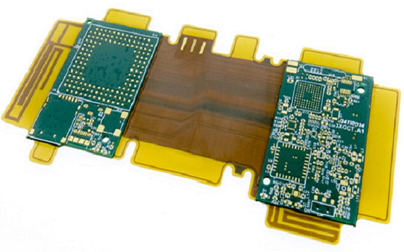
Rigid flex PCB design for manufacturing integrates mechanical bendability, electrical performance, and fabrication feasibility into a unified workflow, ensuring high yield, reliability, and cost efficiency for flexible printed circuit board production. Unlike standard rigid PCB, rigid-flex designs require precise control of bend radius, transition zones, copper routing, and material stack-up to avoid common manufacturing defects like delamination, trace cracking, and warpage. Adhering to IPC-2221 and IPC-6013 standards, this guide provides factory-validated DFM guidelines, real production parameters, and practical solutions for engineers to optimize rigid flex circuit boards for mass production.
Learn more about: Types of Rigid Flex PCB: Complete Classification & Engineering Guide
Key DFM Guidelines for Rigid-Flex PCBs
Bend Radius Management
Bend radius directly determines flexible printed circuit board service life and manufacturing success, with static and dynamic applications requiring distinct design parameters.
- Static Bend (Installation Only): Minimum radius = 10× total flexible thickness; e.g., 0.5mm flex requires ≥5mm radius. Prevents initial stress fractures during assembly.
- Dynamic Bend (Repeated Folding): Minimum radius = 50–100× flexible thickness; 0.5mm flex needs 25–50mm radius. Critical for 10,000+ cycle durability.
- Forbidden Zones: No vias, pads, or components within 3× bend radius of dynamic flex areas. Eliminates stress concentration points.
- Copper Thickness Rule: Use 12–18μm rolled annealed (RA) copper for dynamic bends; 35μm electrolytic (ED) copper for static sections. Balances conductivity and ductility.
Transition Zones
Transition zones between rigid and flex sections are the highest failure risk areas, requiring engineered stress relief and dimensional control.
- Minimum Width: ≥2.5mm for standard designs; ≥4mm for dynamic bending applications. Reduces peel stress during lamination.
- Gradient Thinning: Reduce flexible layer thickness by 50% over 1–2mm at rigid-flex boundaries. Creates a stress buffer zone.
- Symmetrical Transition: Mirror layer structure on both sides of the boundary to prevent warpage during cooling. Maintains structural balance.
- Reinforcement: Add 0.5mm wide copper fillets at all transition corners. Distributes stress away from critical joints.
Copper Routing Techniques
Copper routing in flexible areas requires specialized techniques to prevent fatigue failure while maintaining electrical performance.
Fillets
- Pad Fillets: 45° angled or teardrop-shaped transitions (0.2–0.5mm width) between traces and pads. Eliminates sharp corners that cause stress cracking.
- Via Fillets: 0.3mm minimum radius fillets around all vias in transition zones. Prevents copper separation from dielectric during bending.
- Internal Corners: All internal copper corners in flex areas require ≥0.25mm radius fillets. Reduces acid traps during etching and stress concentration.
Traces
- Orientation: Route traces parallel to bend axis; avoid perpendicular crossings. Minimizes tensile stress during folding.
- Width Consistency: Maintain constant trace width (±10%) throughout flex sections; no abrupt narrowing. Prevents localized current density and stress hotspots.
- Curved Routing: Use continuous arcs (≥1mm radius) instead of 90° angles in dynamic flex zones. Distributes bending stress evenly along trace length.
- Spacing: Minimum trace spacing = 2× trace width in flex areas; e.g., 50μm traces need ≥100μm spacing. Reduces crosstalk and dielectric breakdown risk.
Ground Planes
- Flex Area Grounding: Use grid patterns (30–40% copper coverage) instead of solid planes in dynamic flex zones. Preserves flexibility while maintaining shielding.
- Transition Grounding: Gradually increase copper coverage from 40% (flex) to 100% (rigid) over transition zone. Prevents impedance discontinuity and stress buildup.
- Isolation: Separate rigid and flex ground planes with 0.5mm gap connected by multiple narrow bridges. Controls noise while allowing mechanical movement.
Staggering
- Layer Staggering: Offset trace ends by 0.3–0.5mm between adjacent flex layers. Prevents aligned stress lines that cause layer-to-layer cracking.
- Via Staggering: Stagger vias in transition zones by ≥1mm between layers. Avoids creating vertical stress columns through the stack-up.
- Edge Staggering: Offset flex layer edges by 0.2mm at rigid boundaries. Reduces delamination risk during lamination.
Learn more about: What is Rigid-Flex PCB? A Complete Guide
Stack-up Considerations
Symmetrical vs. Asymmetrical Stack-up
Stack-up symmetry is critical for preventing warpage and ensuring uniform lamination pressure in rigid flex circuit boards.
- Symmetrical Stack-up (Preferred): Mirror layers around central flex core (e.g., Rigid-Flex-Flex-Rigid). Balances thermal expansion coefficients (CTE) during heating/cooling cycles.
- Asymmetrical Stack-up: Flex layers on one side only (Rigid-Flex or Flex-Rigid-Flex). Reduces thickness but increases warpage risk; requires additional stiffeners.
- CTE Matching: Match rigid (FR-4: 12–16 ppm/°C) and flex (PI: 20–25 ppm/°C) materials with low-CTE adhesive (10–15 ppm/°C). Minimizes internal thermal stress.
- Thickness Balance: Keep total rigid thickness ≈ total flex thickness × 2. Prevents uneven pressure distribution during lamination.
Coverlays
Coverlays protect flexible printed circuit board copper traces while maintaining bendability, with strict material and dimensional requirements.
- Material: 20–30μm polyimide (PI) film with 15–25μm acrylic adhesive. Withstands 260°C reflow temperatures and repeated bending.
- Coverage: Extend coverlay 0.2–0.3mm beyond all copper traces in flex areas. Prevents edge exposure and copper oxidation.
- Opening Size: Keep coverlay openings 0.1mm larger than pads; no sharp corners in openings. Reduces stress concentration around component pads.
- Solder Mask Rule: No solder mask on dynamic flex areas; use only PI coverlay. Solder mask is rigid and cracks during bending.
Manufacturing Considerations
| Parameter | Static Rigid-Flex | Dynamic Rigid-Flex |
|---|---|---|
| Min Bend Radius | 10× flex thickness | 50× flex thickness |
| Max Flex Layers | 6–8 layers | 2 layers only |
| Copper Type | ED or RA copper | RA copper exclusively |
| Coverlay Material | PI or solder mask | PI coverlay only |
| Transition Width | ≥2.5mm | ≥4mm |
Lamination Process
Lamination is the most critical manufacturing step for rigid flex PCB, requiring precise control of temperature, pressure, and time.
- Temperature Profile: 185°C–195°C peak temperature with 5–10°C/min ramp rate. Activates adhesive without damaging PI dielectric.
- Pressure Settings: 2.5–3.5 MPa (360–500 psi) for 60–90 minutes. Ensures complete bonding without squeezing out adhesive.
- Vacuum Level: ≤5 mbar (0.07 psi) during lamination. Eliminates air bubbles that cause delamination.
- Cooling Rate: 3–5°C/min under full pressure until ≤50°C. Prevents thermal shock and warpage.
Rigid-flex PCB Material
Material selection directly impacts bendability, reliability, and manufacturing yield for flexible circuit board production.
- Rigid Core: High-Tg FR-4 (Tg ≥130°C), 0.8–1.6mm thickness. Provides stable support for components and heat dissipation.
- Flex Core: 25–50μm polyimide (PI) film, 12–18μm RA copper foil. Balances flexibility and electrical performance.
- Adhesive: Modified epoxy or acrylic, 50–75μm thickness. Bonds rigid and flex layers while absorbing CTE mismatch stress.
- Stiffeners: 0.2–1.0mm FR-4 or 0.1–0.3mm stainless steel for component mounting areas. Prevents flexing under heavy components.
- Surface Finishes: ENIG (2–3μm gold) for flex areas; HASL or OSP for rigid sections. Balances solderability and bend durability.
Core Technical Parameters
- Minimum line width/spacing: 50/50μm (standard), 25/25μm (HDI flexible printed circuit board)
- Minimum via diameter: 0.1mm (laser microvia), 0.3mm (mechanical PTH)
- Flex core thickness: 25–50μm PI; rigid core: 0.8–1.6mm FR-4
- Controlled impedance: ±5% tolerance (50Ω, 90Ω differential)
- Operating temperature: -40°C to +125°C (standard), -55°C to +150°C (automotive)
- Lamination parameters: 190°C, 3MPa, 75 minutes, 3°C/min cooling
- Bend cycle life: 10,000–100,000 cycles (dynamic), 1–50 cycles (static)
- Peel strength: ≥1.2N/mm (IPC-6013 standard)
- DFM yield target: ≥90% for prototype, ≥95% for mass production
Learn more about: What is a Rigid-Flex PCB? Design & Manufacturing Best Practices
Case Study
Project: 6-layer rigid flex PCB for medical wearable device (dynamic wristband application)
- Structure: Symmetrical 2 rigid + 2 flex + 2 flex + 2 rigid stack-up
- Parameters: 35μm RA copper, 0.1mm laser microvias, 50Ω impedance control
- Initial Issues: 30% trace cracking at 5,000 cycles; 20% delamination at transition zones
- Root Causes: 90° trace crossings in bend area; insufficient transition width (1.5mm); CTE mismatch (rigid: 18ppm/°C vs flex: 22ppm/°C)
- Design Corrections: Curved trace routing (1.5mm radius); transition width increased to 4mm; low-CTE adhesive (12ppm/°C) implemented; grid ground planes in flex areas
- Manufacturing Adjustments: Lamination temperature reduced to 180°C; cooling rate slowed to 2°C/min; vacuum hold time extended to 15 minutes
- Final Results: Passed 50,000 bend cycles with zero failures; yield improved from 65% to 94%; delamination eliminated
Common Design Errors
- Incorrect Bend Radius: Using static radius (10× thickness) for dynamic applications, causing 100% early trace failure.
- Sharp 90° Traces in Flex Zones: Creating stress concentration points that fracture copper after 1,000–5,000 cycles.
- Solder Mask on Dynamic Flex Areas: Rigid solder mask cracks during bending, exposing copper to oxidation and corrosion.
- Insufficient Transition Width: <2.5mm width causes delamination during lamination and bending stress failure.
- Vias in Bend Zones: Plating creates rigid columns through flex layers, acting as stress risers that fracture traces.
- Asymmetrical Stack-up Without Stiffeners: Causes severe warpage (>2% twist) during lamination, preventing SMT assembly.
- Solid Ground Planes in Dynamic Flex: Reduces bendability by 60–70%, leading to premature fatigue failure.
Learn more about: How Does Rigid-Flex PCB Work
FAQ
Q: What is the primary IPC standard for rigid flex PCB DFM?
A: IPC-2221 (Generic Standard on Printed Board Design) and IPC-6013 (Qualification and Performance Specification for Flexible Printed Boards) define rigid-flex design and manufacturing requirements.
Q: How many flex layers can be used for dynamic bending applications?
A: A maximum of 2 flex layers is recommended for dynamic bending; additional layers create excessive stress and reduce cycle life.
Q: What is the optimal transition zone width for rigid-flex designs?
A: Minimum 2.5mm for static applications; 4mm or wider for dynamic bending to reduce delamination and stress failure risk.
Q: Why is rolled annealed (RA) copper preferred for dynamic flex areas?
A: RA copper has 30–50% higher ductility than electrolytic (ED) copper, enabling it to withstand repeated bending without cracking or fatigue failure.
If you need professional rigid flex pcb design support or quotation, our team provides free DFM check and fast turnaround.


![Understanding PCB Costs & Pricing [Your Complete Guide]](https://hdicircuitboard.com/wp-content/uploads/elementor/thumbs/Understanding-PCB-Costs-Pricing-Your-Complete-Guide-qzzhe6mcaxuolkux3xalfktgavumi9y1aqfbs9bpv4.webp "Understanding PCB Costs & Pricing [Your Complete Guide]")


