
Flex bend radius is the most critical mechanical parameter in rigid flex PCB design, defining the minimum curvature a flexible printed circuit can withstand without cracking, delamination, or fatigue failure. Governed by IPC-2223 standards, bend radius rules vary by layer count, copper type, and application (static vs dynamic), directly impacting manufacturing yield and long-term reliability. This guide provides factory-validated bend radius formulas, layer-specific thresholds, material requirements, and failure mitigation strategies for rigid flex circuit boards, ensuring designs meet IPC-6013 performance specifications and mass production feasibility.
Learn more about: Rigid Flex PCB Design for Manufacturing
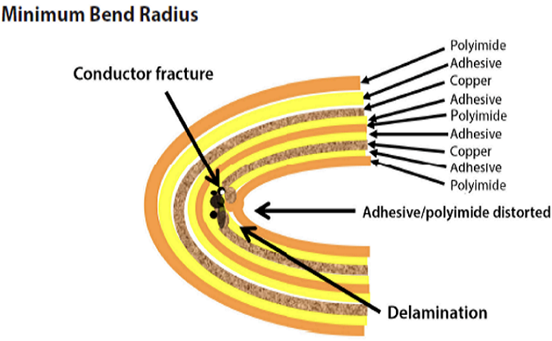
Flexible PCB Bend Radius in Rigid-Flex Design
Core Bend Radius Principle
Bend radius refers to the distance from the bend axis to the inner surface of the flexible circuit, with smaller radii creating higher tensile stress on outer copper layers and compressive stress on inner layers. The neutral axis (center of the flex stack) experiences zero stress, while copper layers farthest from this axis face maximum strain. Rigid-flex designs require balancing mechanical flexibility with electrical integrity, as insufficient bend radius causes 90% of flexible circuit failures during manufacturing or field use.
Stress-Strain Relationship
- Tensile Stress (Outer Layers): Causes copper cracking when strain exceeds 11% (electrolytic copper) or 16% (rolled annealed copper).
- Compressive Stress (Inner Layers): Leads to coverlayer bunching and delamination when radius is too small.
- Neutral Axis Position: Centered in symmetrical stacks; offset in asymmetrical designs, increasing failure risk.
Learn more about: How Does Rigid-Flex PCB Work
Key Bend Radius Rules
Single-Sided Flexible PCB
Single conductive layer on polyimide (PI) substrate, simplest bend configuration with minimal stress risk.
- Minimum Static Bend Radius: 3× total flex thickness (e.g., 0.1mm flex = 0.3mm radius).
- Minimum Dynamic Bend Radius: 20× total flex thickness (e.g., 0.1mm flex = 2mm radius).
- Copper Thickness: 12–18μm RA copper preferred; 35μm ED copper for static only.
- Formula: R = (c/2)×[(100−Eb)/Eb] − D (c=copper thickness, Eb=allowable strain, D=coverlayer thickness).
Double-Sided Flexible PCB
Two copper layers separated by PI dielectric, stress balanced across neutral axis.
- Minimum Static Bend Radius: 4× total flex thickness (e.g., 0.2mm flex = 0.8mm radius).
- Minimum Dynamic Bend Radius: 30× total flex thickness (e.g., 0.2mm flex = 6mm radius).
- Dielectric Thickness: 25–50μm PI; symmetric layer arrangement required.
- Failure Risk: 2× higher than single-sided due to dual copper layers under stress.
Multi-Layer Flexible PCB
3+ copper layers with alternating PI dielectric, highest stress complexity in flex designs.
- Minimum Static Bend Radius: 6× total flex thickness (e.g., 0.3mm flex = 1.8mm radius).
- Minimum Dynamic Bend Radius: 50× total flex thickness (e.g., 0.3mm flex = 15mm radius).
- Max Dynamic Layers: 2 layers; 3+ layers limited to static applications only.
- Layer Staggering: 0.3–0.5mm offset between adjacent layers to avoid aligned stress lines.
Dynamic vs Static Bend Applications
Static Flex (One-Time Installation)
- Definition: Fixed bend during assembly; no repeated movement (e.g., internal device connections).
- Bend Cycles: 1–50 cycles; low fatigue risk.
- Radius Multiplier: 3–6× total flex thickness; cost-effective design option.
- Copper Type: ED or RA copper acceptable; 35μm thickness allowed.
Dynamic Flex (Repeated Bending)
- Definition: Continuous movement during use (e.g., foldable displays, wearable hinges).
- Bend Cycles: 10,000–100,000+ cycles; high fatigue risk.
- Radius Multiplier: 20–100× total flex thickness; strict design constraints.
- Copper Type: RA copper exclusively (30–50% higher ductility than ED copper).
Learn more about: What is Rigid-Flex PCB? A Complete Guide
Key Bend Radius Guidelines (IPC-2223 Standards)
IPC-2223 Core Requirements
IPC-2223 establishes universal bend radius criteria for flexible and rigid-flex PCBs, aligned with IPC-6013 performance standards.
- Standard Reference: IPC-2223 Section 5 – Mechanical Design Considerations for Flexible Circuits.
- Minimum Radius Formula: Rmin = K × T (K=multiplier, T=total flex thickness).
- Class 1 (Consumer): K=3 (static), K=20 (dynamic).
- Class 2 (Industrial): K=4 (static), K=40 (dynamic).
- Class 3 (Aerospace/Medical): K=6 (static), K=100 (dynamic).
| Flex Type | Static Radius (×T) | Dynamic Radius (×T) | Max Layers (Dynamic) |
|---|---|---|---|
| Single-Sided | 3× | 20× | 1 |
| Double-Sided | 4× | 30× | 2 |
| Multi-Layer (3+) | 6× | 50× | 2 |
| One-Time Crease | 1.5× | Not Allowed | 1 |
One-Time Crease (Acute Bend)
Specialized static bend for tight spaces, single-use only with permanent deformation.
- Minimum Radius: 1.5× total flex thickness (e.g., 0.2mm flex = 0.3mm radius).
- Copper Limitation: 12μm RA copper only; no plated vias in bend zone.
- Application: Internal device routing; no repeated movement allowed.
- Failure Risk: 50% higher than standard static bends; factory inspection required.
Designing for Reliability
Material Selection
Material properties directly determine bend tolerance and cycle life in rigid flex circuit boards.
- Flex Core: 25–50μm polyimide (PI) with Tg ≥250°C; low CTE (20–25 ppm/°C).
- Copper Foil:
- RA (Rolled Annealed): 12–18μm, 16% max strain, dynamic bend compatible.
- ED (Electrolytic): 35μm, 11% max strain, static only.
- Coverlayer: 20–30μm PI with 15–25μm acrylic adhesive; extends 0.2–0.3mm beyond traces.
- Adhesive: Modified epoxy, 50–75μm thickness, CTE 10–15 ppm/°C for CTE matching.
Avoid Vias/Pads in Bend Zones
Vias and pads create rigid stress risers that fracture copper during bending.
- Exclusion Zone: No vias/pads within 3× bend radius of dynamic flex areas.
- Via Placement: Minimum 1mm distance from rigid-flex transition zones.
- Pad Restrictions: No component pads in bend regions; use surface mounts on rigid sections.
- Failure Mechanism: Plated vias create vertical rigid columns, causing 100% early failure in dynamic bends.
Trace Design
Trace geometry in flex zones must minimize stress concentration while maintaining electrical performance.
- Orientation: Route traces parallel to bend axis; perpendicular crossings increase stress by 300%.
- Width: Minimum 50μm width; consistent width (±10%) throughout bend zone.
- Corners: All internal corners ≥0.25mm radius; no 90° angles in dynamic flex.
- Fillets: 0.2–0.5mm teardrop fillets at trace-pad junctions; reduces stress by 50%.
Copper Planes
Solid copper planes in flex zones reduce bendability and increase fatigue risk.
- Dynamic Flex: Grid planes (30–40% copper coverage); maintains shielding while preserving flexibility.
- Static Flex: Solid planes allowed; use 50% copper weight to reduce stiffness.
- Transition: Gradual coverage increase (40% to 100%) over 2mm at rigid-flex boundaries.
Transition Zones
Rigid-flex boundaries are high-stress areas requiring engineered stress relief.
- Width: Minimum 2.5mm (static); 4mm (dynamic).
- Gradient Thinning: Reduce flex thickness by 50% over 1–2mm at boundaries.
- Symmetry: Mirror layer structure on both sides to prevent warpage.
- Copper Fillets: 0.5mm wide fillets at transition corners; distributes stress evenly.
Example Calculation
Static Bend (Double-Sided Flex)
- Parameters: Total flex thickness (T) = 0.2mm (25μm PI + 18μm Cu + 25μm PI + 18μm Cu).
- IPC-2223 Class 2: Static radius multiplier = 4×.
- Minimum Radius: 4 × 0.2mm = 0.8mm.
- Coverlayer: 25μm PI, extends 0.25mm beyond traces.
- Copper: 18μm RA copper, 16% max strain capacity.
Dynamic Bend (Single-Sided Flex)
- Parameters: Total flex thickness (T) = 0.1mm (25μm PI + 12μm Cu + 25μm coverlayer).
- IPC-2223 Class 3: Dynamic radius multiplier = 100×.
- Minimum Radius: 100 × 0.1mm = 10mm.
- Bend Cycles: Target 50,000+ cycles for wearable application.
- Copper: 12μm RA copper only; ED copper prohibited.
Why Bend Radius Matters
Coverlayer Bunching
Insufficient radius causes coverlayer compression, leading to wrinkling and delamination.
- Mechanism: Inner coverlayer compresses beyond elastic limit, creating permanent folds.
- Impact: Exposes copper to oxidation; reduces insulation resistance by 80%.
- Prevention: Adhere to minimum radius; use thinner coverlayers (20μm) for tight bends.
Copper Fatigue/Breaking
Excessive tensile stress on outer copper layers causes microcracks and open circuits.
- Mechanism: Repeated bending causes crack propagation at stress concentration points.
- Threshold: RA copper fails at >16% strain; ED copper at >11% strain.
- Impact: Intermittent or permanent signal failure; 90% of dynamic flex failures are copper-related.
Delamination
CTE mismatch and insufficient radius cause layer separation at rigid-flex boundaries.
- Mechanism: Thermal cycling and bending stress exceed adhesive peel strength (≥1.2N/mm per IPC-6013).
- Impact: Electrical isolation loss; structural failure under vibration.
- Prevention: CTE-matched materials; sufficient transition width; controlled lamination (190°C, 3MPa).
Design Tips for Proper Bend Radius
Calculate Total Thickness
Include all layers (copper, dielectric, coverlayer) when computing bend radius.
- Formula: T = Cu1 + D1 + Cu2 + D2 + CL (Cu=copper, D=dielectric, CL=coverlayer).
- Common Mistake: Excluding coverlayer thickness, leading to undersized radius.
Use RA Copper
Specify rolled annealed copper for all dynamic flex applications.
- Ductility: 30–50% higher than ED copper; withstands 50,000+ cycles.
- Cost Premium: 15–20% vs ED copper; justified by 10× longer cycle life.
Staggered Traces
Offset trace ends between layers to avoid aligned stress lines.
- Offset: 0.3–0.5mm between adjacent layers; reduces crack propagation risk.
Routing Best Practices
- Maintain Distance: Keep bend zones 5mm away from connectors and components.
- Smooth Arcs: Use continuous arcs (≥1mm radius) instead of sharp angles.
- Test Early: Perform MIT bend testing (IPC-TM-650 2.4.30) on prototypes.
Core Technical Parameters
- Minimum static bend radius: 3× flex thickness (single-sided), 4× (double-sided), 6× (multi-layer)
- Minimum dynamic bend radius: 20× flex thickness (single-sided), 30× (double-sided), 50× (multi-layer)
- Copper thickness: 12–18μm RA (dynamic), 35μm ED (static only)
- Coverlayer thickness: 20–30μm PI; 15–25μm acrylic adhesive
- Transition zone width: ≥2.5mm (static), ≥4mm (dynamic)
- Maximum dynamic flex layers: 2 layers (IPC-2223)
- Allowable copper strain: 16% (RA), 11% (ED)
- Bend cycle life: 10,000–100,000 (dynamic), 1–50 (static)
Case Study
Project: 4-layer rigid flex PCB for foldable smartphone hinge (dynamic 180° bending)
- Structure: Symmetrical 2 rigid + 2 flex layers; 0.2mm total flex thickness.
- Parameters: IPC-2223 Class 3, 100× dynamic radius (20mm), 12μm RA copper.
- Initial Issues: 40% trace cracking at 10,000 cycles; 25% delamination at transition zones.
- Root Causes**: Perpendicular trace crossings in bend zone; insufficient transition width (1.5mm); ED copper used in dynamic layers.
- Design Corrections**: Parallel trace routing; transition width increased to 4mm; RA copper implemented; grid ground planes in flex areas.
- Manufacturing Adjustments**: Lamination temperature reduced to 180°C; vacuum hold time extended to 15 minutes; post-lamination stress relief bake (120°C, 60min).
- Final Results**: Passed 100,000 bend cycles with zero failures; yield improved from 58% to 93%; delamination eliminated.
Common Design Errors
- Undersized Bend Radius: Using static multipliers (3×) for dynamic applications, causing 100% early copper failure.
- Vias in Bend Zones: Plated vias create stress risers, fracturing traces after 5,000–10,000 cycles.
- ED Copper in Dynamic Flex: Electrolytic copper’s low ductility (11% max strain) leads to rapid fatigue failure.
- Solid Ground Planes in Dynamic Zones: Reduces bendability by 60%, causing premature cracking.
- Insufficient Transition Width: <2.5mm width causes delamination during lamination and bending.
- 90° Trace Angles in Flex: Sharp corners create stress concentrations, initiating cracks at 1,000–3,000 cycles.
- Ignoring Coverlayer Thickness: Excluding coverlayer from total thickness calculation results in undersized radius.
Learn more about: What is a Rigid-Flex PCB? Design & Manufacturing Best Practices
FAQ
Q: What is the primary IPC standard for flex bend radius in rigid flex PCB?
A: IPC-2223 Section 5 defines bend radius rules, with IPC-6013 specifying performance requirements for flexible and rigid-flex circuits.
Q: How many flex layers can be used for dynamic bending?
A: IPC-2223 allows a maximum of 2 flex layers for dynamic bending; additional layers create excessive stress and reduce cycle life.
Q: What is the difference between RA and ED copper for flex bends?
A: RA (Rolled Annealed) copper has 30–50% higher ductility (16% max strain) than ED (Electrolytic) copper (11% max strain), making it suitable for dynamic bending applications.
Q: Why are vias prohibited in dynamic bend zones?
A: Plated vias create rigid vertical columns through flex layers, acting as stress risers that fracture copper traces during repeated bending, leading to early failure.
If you need professional rigid flex pcb design support or quotation, our team provides free DFM check and fast turnaround.


![Understanding PCB Costs & Pricing [Your Complete Guide]](https://hdicircuitboard.com/wp-content/uploads/elementor/thumbs/Understanding-PCB-Costs-Pricing-Your-Complete-Guide-qzzhe6mcaxuolkux3xalfktgavumi9y1aqfbs9bpv4.webp "Understanding PCB Costs & Pricing [Your Complete Guide]")


