
High speed rigid flex PCB design demands precise control of impedance continuity, layer stackup symmetry, flex mechanical limits and EMI suppression across rigid and flexible printed circuit sections. Operating above 10Gbps introduces signal reflection, crosstalk and bend-induced dielectric variation that degrade signal integrity in rigid flex circuit boards. Compliant with IPC-2223 and IPC-6013 standards, these design guidelines integrate factory validated routing rules, material selection parameters and flex-to-rigid transition control to maintain ±5% impedance tolerance, controlled bend radius and consistent return paths throughout flexible circuit board layouts. Every tip aligns engineering design intent with actual fabrication process limits to eliminate rework and preserve long-term mechanical reliability.
Learn more about: Impedance Control in Rigid Flex PCB: Design, Stack-up & Manufacturing Rules
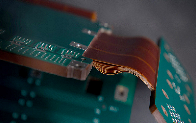
High-Speed Routing and Impedance Control
Controlled Impedance in Flex Regions
Controlled impedance forms the foundation of high speed rigid flex PCB performance, with standard targets set at 50Ω single-ended and 100Ω differential across all flexible printed circuit segments.
- Impedance tolerance maintains ±5% for standard high-speed designs and ±3% for 25Gbps+ premium applications following IPC-2221 calculation protocols.
- Flex region dielectric thickness ranges from 25μm to 50μm for polyimide substrates, directly altering trace width requirements by 8% to 12% compared to rigid FR-4 sections.
- Impedance recalculation is mandatory at every flex-to-rigid boundary due to Dk variance between PI (3.2–3.5) and high-Tg FR-4 (4.0–4.4).
- Bend deformation can shift impedance by 4% to 7% in dynamic flex zones, requiring pre-routing trace width compensation during layout.
Differential Pairs Routing Rules
Differential pair management prevents skew and crosstalk in high speed rigid flex PCB layouts within flexible circuit board structures.
- Maintain fixed pair spacing of 0.15mm to 0.25mm across rigid and flex areas with zero width variation.
- Limit length skew below 5ps per meter to preserve phase alignment for high-speed serial interfaces.
- Route differential pairs entirely on inner flex layers to avoid outer layer mechanical strain altering impedance values.
- Separate unrelated high-speed differential routes by a minimum 3x trace width distance to suppress crosstalk under 20dB.
Layer Stackup and Materials
Minimal Layers & Symmetry
Layer stackup symmetry eliminates warpage, layer shift and impedance skew in multi-layer rigid flex circuit boards.
- Adopt symmetrical stackup architecture placing flex layers on the neutral mechanical axis to reduce bending stress by over 60%.
- Restrict unnecessary layer addition; minimal layer design lowers lamination thickness variation and stabilizes Dk consistency.
- Match dielectric thickness equally above and below each flex core to maintain uniform impedance across the entire flexible printed circuit.
- Asymmetrical stackup is only permissible for static non-bending applications with relaxed ±7% impedance tolerance.
Adhesiveless Materials Selection
Copper and dielectric material choice directly impacts signal integrity and cycle life of flexible circuit board structures.
- Adhesiveless polyimide features Dk of 3.2±0.05 with thickness tolerance ±5%, outperforming adhesive-based PI in high precision impedance control.
- RA rolled copper of 12μm thickness is standard for dynamic flex routes, while 18μm RA copper suits static bending zones.
- High-Tg FR-4 rated 170°C minimum reduces thermal Dk drift under 85°C operating temperature in rigid sections.
- Low-loss prepreg with Dk 3.5±0.04 minimizes signal attenuation below 0.15dB/cm at 10GHz for high speed rigid flex PCB layouts.
Learn more about: Rigid Flex PCB Design for Manufacturing
Routing in Flex Areas
Perpendicular & Curved Traces
Routing geometry directly affects mechanical fatigue and impedance stability inside flexible zones.
- Route all high-speed traces perpendicular to the bending axis to avoid longitudinal crack formation during repeated flexing.
- Adopt curved traces with 0.5mm minimum arc radius; eliminate 90-degree angles that create stress concentration and impedance discontinuity.
- Staggered traces across adjacent flex layers prevent overlapping dielectric compression that distributes uniform impedance deviation.
- Maintain fixed trace width of 0.18mm to 0.22mm for 50Ω routes without tapering inside continuous flex regions.
Avoid Bending Areas Restrictions
High speed rigid flex PCB routing must exclude sensitive structures from active bend zones.
- Place no component pads, plated vias or dense copper fills within any dynamic bending region of the flexible printed circuit.
- Keep high-speed signal routes confined to inner flex layers while reserving outer flex layers for low-speed control lines only.
- Maintain 2mm clear buffer zone around all rigid-flex boundaries free of dense routing clusters.
- Restrict trace density below 65% inside flex zones to preserve structural flexibility and uniform dielectric compression.
Hatched Ground Planes & Return Paths
Hatched Ground Planes Implementation
Hatched ground planes balance EMI shielding and mechanical flexibility unique to flexible circuit board designs.
- Set hatch pattern copper coverage at 30% to 40% with 0.2mm line width and 0.4mm spacing for standard flex zones.
- Hatched structures increase baseline impedance by 5% to 8%, requiring trace width adjustment by +10% for target impedance matching.
- Gradually transition hatch coverage from 40% in flex to 100% solid plane in rigid sections over a 2mm linear zone.
- Solid ground planes inside flex areas cause up to 10% impedance shift during bending and reduce flex cycle life significantly.
Return Paths & Ground Stitching
Continuous return paths stabilize signal integrity and suppress EMI across rigid flex circuit boards.
- Route high-speed signals directly adjacent to dedicated ground reference planes to create uninterrupted microstrip or stripline return paths.
- Apply ground stitching vias spaced 1.0mm to 1.5mm apart along flex-to-rigid transition boundaries to close return path gaps.
- Eliminate split ground planes under high-speed routes; discontinuities introduce return path disruption and EMI radiation.
- Anchor stitching vias outside active bend zones to avoid mechanical stress on plated barrel structures.
Learn more about: Types of Rigid Flex PCB: Complete Classification & Engineering Guide
Mechanical and Flex Reliability
Bend Radius Compliance
Bend radius parameters define mechanical lifespan and electrical stability for flexible printed circuit layouts.
- Static bend radius minimum set at 6x total board thickness; dynamic frequent bending requires 10x board thickness per IPC-2223.
- Standard 0.1mm flex stack requires minimum 1.0mm dynamic bend radius to prevent copper fatigue after 100k flex cycles.
- Reduce trace density by 20% inside tight bend radius zones to distribute stress evenly across substrate and copper layers.
- Avoid placing differential pairs directly along maximum bend stress lines to prevent skew drift over time.
Flex-to-Rigid Transition Design
Transition zone control eliminates impedance discontinuity and mechanical failure at rigid flex boundaries.
- Maintain minimum transition length of 2.5mm for static applications and 4mm for dynamic bending layouts.
- Avoid Rigid Boundaries placement of plated vias, component footprints and dense copper within 1mm of transition edges.
- Apply gradual layer tapering across transition zones rather than abrupt layer termination to balance dielectric loading.
- Use copper fillets of 0.3mm width at trace plane junctions to reduce current crowding and mechanical stress concentration.
Via and Pad Management
Via Placement & Minimize Vias
Via usage directly introduces parasitic capacitance and inductance that distort high-speed signal integrity.
- Minimize via count on all 10Gbps+ routes; each via adds 0.2pF parasitic capacitance triggering minor impedance deviation.
- Restrict all plated vias outside flex zones entirely; deploy laser microvias of 0.1mm diameter only within rigid sections.
- Staggered vias across adjacent layers prevent vertical stress columns that warp layer stackup and shift impedance values.
- Anchor Vias positioned outside bend areas reinforce layer bonding without interfering with flexible movement.
Use Teardrops & Pad Rules
Teardrop implementation improves thermal and mechanical reliability on rigid flex circuit board layouts.
- Apply 45-degree teardrops at trace-to-pad junctions in transition zones to reduce stress cracking during flex cycling.
- Limit pad size enlargement in flex regions to avoid excess copper mass creating localized rigid spots.
- Maintain 0.2mm minimum clearance between pad edges and bend zone perimeters to preserve substrate flexibility.
Learn more about: What is Rigid-Flex PCB? A Complete Guide
EMI Shielding & Design for Manufacturing
EMI Shielding Best Practices
EMI control integrates grounding, routing separation and plane structure for high speed rigid flex PCB performance.
- Isolate high-speed differential routes from power traces by minimum 3x trace width distance to reduce capacitive crosstalk.
- Use continuous hatched ground planes as primary shielding inside flex regions and solid planes in rigid segments.
- Align ground stitching density higher along edge routes to suppress edge radiation from flexible printed circuit borders.
- Keep clock routes separated from data lines by dedicated ground barriers to lock EMI emission below regulatory limits.
DFM & Early Manufacturer Collaboration
Design for Manufacturing aligns layout parameters with actual fabrication limits to maintain yield and performance.
- Share finalized layer stackup and impedance requirements in early design stages to validate material Dk and thickness availability.
- Follow factory minimum line width 0.05mm and spacing 0.05mm for high-density flexible circuit board production.
- Confirm lamination pressure parameters of 3MPa and temperature 185°C to avoid layer shift affecting impedance consistency.
- Integrate impedance test coupons on every panel covering rigid, flex and transition zones for TDR validation per IPC-TM-650.
Core Technical Parameter Specifications
- Standard target impedance: 50Ω single-ended, 100Ω differential
- Impedance tolerance: ±5% standard, ±3% high-speed 25Gbps+
- Flex dielectric thickness: 25μm–50μm; rigid core thickness: 0.8mm–1.6mm
- Trace width range for 50Ω routes: 0.18mm–0.22mm
- Minimum dynamic bend radius: 10x overall board thickness
- Transition zone minimum length: 2.5mm static, 4mm dynamic
- Hatch ground coverage: 30%–40% with 0.2mm line / 0.4mm space
- Ground stitching via pitch: 1.0mm–1.5mm along transition boundaries
- Allowable differential skew: under 5ps per meter
- Lamination production parameters: 185°C, 3MPa, 75 minute cycle
Material & Structure Comparison Table
| Design Parameter | Adhesiveless Flex Material | Adhesive-Based Flex Material |
|---|---|---|
| Dielectric Constant Dk | 3.2±0.05 | 3.4±0.10 |
| Impedance Tolerance Capability | ±3% | ±5% |
| Bend Cycle Lifespan | Over 150,000 cycles | 80,000–100,000 cycles |
| Trace Width Compensation Need | Under 5% | 8%–12% |
| High-Speed Signal Loss at 10GHz | Below 0.15dB/cm | 0.20–0.25dB/cm |
Case Study
Project: 8-layer high speed rigid flex PCB for industrial edge computing flexible circuit board
- Structure: Symmetrical 4 rigid inner layers paired with 2 central flex layers, total board thickness 0.9mm
- Key Parameters: 100Ω differential high-speed lanes at 12Gbps, ±5% impedance tolerance, adhesiveless PI dielectric, 12μm RA copper
- Initial Field Issues: 12% impedance deviation at transition zones, signal skew reaching 12ps/m, 6% production yield loss from bend cracking
- Root Causes: Asymmetric local routing near boundaries, solid ground planes in flex sections, transition length limited to 1.8mm, non-perpendicular trace routing across bend axis
- Design Optimizations: Extended transition zone to 4mm, replaced solid planes with 35% hatched ground structure, rerouted all high-speed traces perpendicular to bend axis, added staggered layer pairing and ground stitching at 1.2mm pitch
- Manufacturing Adjustments: Implemented bookbinding lamination process, laser trace etching for ±0.02mm width control, TDR full panel testing at 25°C and 85°C
- Final Outcome: Impedance deviation controlled within ±4.2%, differential skew reduced to 4ps/m, production yield improved from 94% to 98.5%, flex cycle lifespan stabilized above 120,000 cycles
Common Design Errors
- Applying identical trace width across rigid and flex regions without recalculating impedance for Dk and thickness differences
- Plating vias inside dynamic bend zones causing barrel stress and gradual impedance drift over flex cycles
- Using solid ground planes in flex areas creating excessive impedance shift during mechanical bending
- Designing asymmetrical layer stackup leading to lamination warpage and uneven impedance distribution
- Routing high-speed traces parallel to bend axis resulting in copper cracking and signal integrity degradation
- Setting transition zone length below 2.5mm generating sharp impedance discontinuity and signal reflection
- Omitting ground stitching along flex-to-rigid boundaries creating broken return paths and increased EMI radiation
- Overlooking teardrop structures at trace-pad junctions leading to fatigue failure after repeated flexing
FAQ
Q: What is the optimal layer stackup rule for high speed rigid flex PCB layouts?
A: Symmetrical stackup placing all flex layers on the mechanical neutral axis remains optimal, maintaining dielectric balance and limiting impedance variation within ±5% while maximizing bend cycle life per IPC-2223 specifications.
Q: Why are hatched ground planes preferred over solid planes in flexible printed circuit designs?
A: Hatched ground planes preserve mechanical flexibility while retaining 80% shielding efficiency, limiting bend-induced impedance shift to under 8% compared to up to 10% deviation from solid ground structures inside flex zones.
Q: What minimum bend radius should be followed for dynamic high speed rigid flex PCB applications?
A: Dynamic frequent bending requires a minimum bend radius equal to 10x total board thickness, while static non-moving flex sections safely follow a 6x thickness rule to avoid copper fatigue and impedance drift.
Q: How can engineers minimize signal skew on differential pairs in rigid flex circuit boards?
A: Maintain fixed trace spacing throughout rigid and flex segments, route pairs on inner flex layers, control length skew under 5ps per meter, and separate adjacent signal routes by 3x trace width to suppress crosstalk and timing deviation.
If you need professional rigid flex pcb design support or quotation, our team provides free DFM check and fast turnaround.


![Understanding PCB Costs & Pricing [Your Complete Guide]](https://hdicircuitboard.com/wp-content/uploads/elementor/thumbs/Understanding-PCB-Costs-Pricing-Your-Complete-Guide-qzzhe6mcaxuolkux3xalfktgavumi9y1aqfbs9bpv4.webp "Understanding PCB Costs & Pricing [Your Complete Guide]")


