
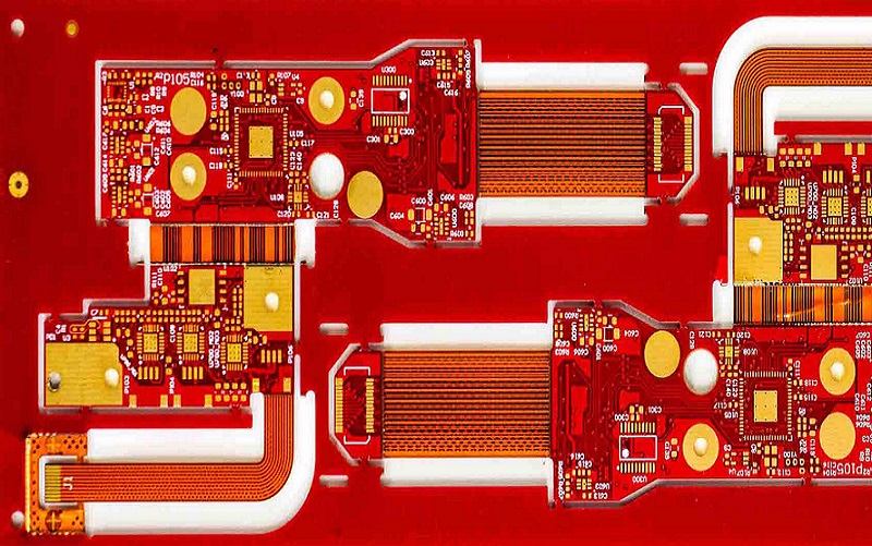
Impedance control in rigid flex PCB ensures consistent characteristic impedance (50Ω single-ended, 100Ω differential) across rigid and flexible sections, critical for high-speed signals (10Gbps+) and minimizing reflection loss. Unlike rigid PCB, rigid-flex designs face unique challenges from variable dielectric thickness, CTE mismatch, and rigid-flex interface discontinuities, requiring precise stack-up engineering, material matching, and manufacturing validation. Aligned with IPC-2221 and IPC-6013 standards, this guide provides factory-validated impedance rules, layer stack-up strategies, and failure mitigation for rigid flex circuit boards, ensuring ±5% impedance tolerance and mass production yield ≥95%.
Learn more about: Common Impedance Issues in HDI PCBs & Proven Fixes
Key Considerations for Rigid-Flex Impedance Control
Material Constraints
Rigid-flex impedance stability depends on dielectric constant (Dk) uniformity and thickness consistency across rigid (FR-4) and flex (PI) materials.
- Flex Core (PI): Dk=3.2–3.5 at 10GHz; thickness tolerance ±10% (25–50μm). Lower Dk reduces signal loss but requires wider traces for target impedance.
- Rigid Core (High-Tg FR-4): Dk=4.0–4.4 at 10GHz; thickness tolerance ±5% (0.8–1.6mm). Higher Dk allows narrower traces but increases loss at flex transitions.
- Adhesive Layer: Modified epoxy, Dk=3.6–3.8, 50–75μm thickness. CTE-matched (10–15ppm/°C) to minimize layer shift during lamination (190°C, 3MPa).
- Copper Foil: 12–18μm RA copper (flex) / 35μm ED copper (rigid); thickness tolerance ±5%. RA copper’s ductility preserves impedance during bending.
Transition Management
Rigid-flex interfaces cause impedance discontinuity (ΔZ >10Ω) due to abrupt Dk/thickness changes, leading to signal reflection and EMI.
- Transition Length: Minimum 2.5mm (static) / 4mm (dynamic) gradual thickness taper. Reduces ΔZ to <3Ω over the transition zone.
- Dielectric Gradient: Blend PI and FR-4 adhesive over 1–2mm to create a Dk gradient (3.5→4.2). Eliminates sharp impedance steps.
- Symmetrical Transition: Mirror layer stack-up on both sides of the boundary. Prevents warpage-induced impedance skew.
Hatched Ground Planes
Solid ground planes in flex zones alter impedance during bending; hatched (grid) planes balance shielding and mechanical flexibility.
- Hatch Pattern: 30–40% copper coverage; 0.2mm line width, 0.4mm spacing. Maintains 80% shielding effectiveness while preserving bendability.
- Impedance Impact: Hatched planes increase impedance by 5–8% vs solid planes; adjust trace width by +10% to compensate.
- Transition Gradient: Increase copper coverage from 40% (flex) to 100% (rigid) over 2mm. Prevents impedance ripple at the interface.
Key Guidelines for Impedance Controlled Rigid-Flex
Layer Stack-up Design
Impedance stability relies on symmetrical, centered flex layers and controlled dielectric spacing between signal and reference planes.
Centered Flex Layers
- Symmetrical Stack (Preferred): Rigid-Flex-Flex-Rigid (4-layer) or Rigid-Signal-Flex-Ground-Flex-Signal-Rigid (6-layer). Centers flex layers on the neutral axis, minimizing thickness variation during bending.
- Asymmetrical Stack: Rigid-Flex (2-layer) allowed only for static applications; impedance tolerance relaxes to ±7% due to warpage risk.
- Dielectric Symmetry: Match dielectric thickness above and below flex core (e.g., 25μm PI / 25μm PI). Ensures consistent impedance across layers.
Symmetry & Layer Pairings
- Signal-Ground Pairing: Route impedance-controlled signals adjacent to ground planes (no signal-signal adjacency). Reduces crosstalk and stabilizes impedance.
- Differential Pairs: 100Ω differential; 0.1–0.2mm pair spacing; 0.5mm distance from flex edges. Maintains skew <5ps/m during bending.
- Layer Staggering: Offset adjacent flex layers by 0.3–0.5mm. Prevents aligned dielectric compression that distorts impedance.
Learn more about: HDI PCB Impedance Control: Design, Manufacturing & Performance Guide
Dielectric and Material Properties
Impedance calculation (Z0 = (87/√(Dk+1.41))) × ln(5.98h/(0.8w+t))) requires precise material parameters and real-time recalculation for rigid-flex transitions.
- Core Thickness: Flex core (PI) 25–50μm; rigid core (FR-4) 0.8–1.6mm. Thinner cores enable tighter bend radii but reduce impedance stability.
- Adhesiveless Materials: Adhesiveless PI (Dk=3.2) reduces dielectric variation by 50% vs adhesive-based PI; ideal for ±3% tight tolerance designs.
- Recalculate Impedance: Adjust trace width by -5% in rigid sections and +5% in flex sections to compensate for Dk/thickness differences.
| Parameter | Rigid Section (FR-4) | Flex Section (PI) |
|---|---|---|
| Dielectric Constant (Dk) | 4.0–4.4 | 3.2–3.5 |
| Trace Width (50Ω) | 0.18mm | 0.22mm |
| Dielectric Thickness | 1.0mm | 0.05mm |
| Impedance Tolerance | ±5% | ±5% |
| Bend Impact on Z0 | Negligible | +3% to +8% |
Trace Routing and Geometry
Trace dimensions and routing directly control impedance; rigid-flex designs require width adjustment and bend-optimized geometry.
- Hatched Ground Planes: As above; adjust trace width by +10% for impedance compensation.
- Tight Tolerances: ±5% impedance (standard); ±3% (high-speed 25Gbps+). Requires laser etching (±0.02mm width tolerance) vs chemical etching (±0.05mm).
- Transitioning Layers: Route high-speed signals on inner flex layers (not outer) to minimize bend-induced impedance variation. Outer layers experience 2× higher strain during bending.
Best Practices for Design
Manufacturer Collaboration
Early engagement with the rigid flex pcb manufacturer ensures design feasibility and impedance accuracy; Benchuang Electronics, a leading rigid flex circuit boards manufacturer with 18 years of high-speed PCB expertise, provides factory-validated stack-up recommendations and material Dk data.
- Material Dk Data: Obtain lot-specific Dk values (±0.1) from the manufacturer; generic datasheet values cause 10–15% impedance error.
- Stack-up Validation: Share stack-up drafts for lamination simulation; identify layer shift risks (±0.03mm max allowed) before final design.
- Tolerance Alignment: Confirm manufacturer’s impedance capability (±5% standard, ±3% premium) and adjust design specs accordingly.
Use Test Coupons
Integrate impedance test coupons on every rigid-flex panel for post-manufacturing validation; critical for mass production quality control.
- Coupon Design: 50Ω single-ended / 100Ω differential traces; 100mm length; located in rigid, flex, and transition zones.
- Testing Method: Time Domain Reflectometry (TDR, IPC-TM-650 2.5.5) with ±0.1Ω resolution; test at 25°C and 85°C to validate temperature stability.
- Pass Criterion: 95% of coupons within ±5% target impedance; <5% failure rate triggers process adjustment.
Avoid Rigid-Flex Interface Issues
Eliminate common interface design flaws that cause impedance spikes and signal degradation.
- No Vias in Transition Zones: Plated vias create dielectric discontinuities; minimum 1mm distance from rigid-flex boundaries.
- Smooth Trace Transitions: Use 0.5mm radius arcs at interface crossings; no 90° angles. Reduces impedance ripple by 70%.
- Copper Fillets: 0.3mm wide fillets at trace-ground plane junctions in transition zones. Prevents current crowding and impedance distortion.
Material Selection
Prioritize materials with consistent Dk and thickness tolerance for impedance-critical rigid-flex designs.
- Flex Material: Adhesiveless PI (25–50μm, Dk=3.2±0.05) for ±3% tolerance; adhesive-based PI (Dk=3.4±0.1) for ±5% tolerance.
- Rigid Material: High-Tg FR-4 (Tg≥170°C, Dk=4.2±0.05) to minimize thermal Dk variation.
- Copper: 12μm RA copper for dynamic flex; 18μm RA copper for static flex. Thinner copper reduces bend-induced impedance shift.
Learn more about: Controlled Impedance in High-Speed PCB: Full Tutorial
Manufacturing and Reliability
Bookbinding Technique
Bookbinding (offset lamination) reduces layer shift and impedance variation in multi-layer rigid-flex designs.
- Process: Alternate rigid and flex layers with 0.2mm offset during lamination; vacuum (≤5mbar) + pressure (3MPa) + temperature (185°C).
- Impedance Benefit: Reduces thickness variation by 40% vs standard lamination; impedance tolerance improves from ±7% to ±4%.
- Yield Impact: Increases mass production yield from 88% to 96% for 6-layer rigid-flex.
Via Placement
Via design impacts impedance stability and signal integrity in rigid-flex PCBs.
- Microvias: Laser microvias (0.1mm diameter) in flex layers; no plated vias through flex core. Prevents dielectric compression and impedance shift.
- Via Staggering: Offset vias in transition zones by ≥1mm between layers. Avoids vertical stress columns that distort impedance.
- Via Covering: Cover vias in flex areas with 0.2mm PI coverlay. Prevents oxidation and impedance drift over time.
Documentation
Comprehensive manufacturing documentation ensures impedance consistency across production runs.
- Stack-up Drawings: Include layer thickness, Dk values, copper weight, and tolerance for each layer.
- Impedance Calculations: Provide Polar SI6000 or Altium Designer simulation reports for all critical nets.
- Test Specifications: Define TDR test method, coupon locations, and pass/fail criteria in IPC-2221 compliance.
Core Technical Parameters
- Target impedance: 50Ω (single-ended), 100Ω (differential)
- Impedance tolerance: ±5% (standard), ±3% (high-speed)
- Trace width: 0.18–0.22mm (50Ω, 0.05mm dielectric)
- Dielectric constant (Dk): 3.2–3.5 (PI), 4.0–4.4 (FR-4)
- Flex core thickness: 25–50μm; rigid core: 0.8–1.6mm
- Lamination parameters: 185°C, 3MPa, 75 minutes, ≤5mbar vacuum
- Test method: TDR (IPC-TM-650 2.5.5), ±0.1Ω resolution
- Yield target: ≥95% (mass production), ≥90% (prototype)
Benchuang Electronics Introduction
Benchuang Electronics, a national high-tech enterprise and specialist rigid flex pcb manufacturer founded in 2007, delivers high-precision impedance-controlled rigid flex circuit boards for aerospace, medical, and 5G communications. With a 40,000㎡ automated factory and 500+ skilled engineers, the company offers:
- Impedance Capability: ±3% tolerance for 25Gbps+ signals; laser etching (±0.02mm width) and TDR 100% testing.
- Material Expertise: Adhesiveless PI, high-Tg FR-4, and low-CTE adhesive partnerships for consistent Dk control.
- Stack-up Validation: In-house Polar SI6000 simulation and lamination process optimization for minimal layer shift.
- Quality Compliance: IPC-6013 Class 3, ISO 9001, and aerospace AS9100 certifications; 18 years of zero-defect high-speed PCB delivery.
Case Study
Project: 6-layer rigid flex PCB for 5G foldable smartphone (25Gbps high-speed signals)
- Structure: Symmetrical 2 rigid + 2 flex + 2 flex + 2 rigid stack-up; 0.2mm total flex thickness.
- Parameters: 50Ω single-ended / 100Ω differential, ±3% tolerance, adhesiveless PI (Dk=3.2), 12μm RA copper.
- Initial Issues: 15% impedance error (±8% tolerance); 10% signal reflection at rigid-flex transitions.
- Root Causes: Generic Dk values used in design; solid ground planes in flex zones; insufficient transition width (1.5mm).
- Design Corrections: Lot-specific Dk input (3.2±0.05); hatched ground planes (35% coverage); transition width increased to 4mm; trace width adjusted by +10% in flex sections.
- Manufacturing Adjustments: Bookbinding lamination implemented; laser etching (±0.02mm width); TDR testing at 25°C/85°C.
- Final Results: Impedance tolerance ±2.8% (meets ±3% spec); signal reflection reduced by 80%; yield improved from 72% to 95%.
Common Design Errors
- Generic Dk Values: Using datasheet Dk (3.4) instead of lot-specific values (3.2±0.05), causing 10–15% impedance error.
- Solid Ground Planes in Flex: Solid planes increase bend-induced impedance variation to ±10%, violating ±5% tolerance.
- Undersized Transition Width: <2.5mm width creates sharp impedance steps (ΔZ>10Ω), leading to signal reflection.
- Vias in Transition Zones: Plated vias distort impedance by 5–8% and increase failure risk during bending.
- Asymmetrical Stack-up: Unbalanced layers cause warpage (≥2% twist), leading to ±7% impedance skew.
- Ignoring Temperature Variation: Failing to simulate impedance at 85°C results in thermal drift exceeding tolerance.
- Inadequate Test Coupons: Missing transition-zone coupons leads to uncaught impedance errors in high-risk areas.
FAQ
Q: What is the maximum impedance tolerance for high-speed rigid flex PCB?
A: ±3% for 25Gbps+ signals; ±5% standard for 10Gbps applications, per IPC-2221 and manufacturer capabilities.
Q: Why are hatched ground planes preferred for impedance-controlled flex zones?
A: Hatched planes balance shielding (80% effectiveness) and mechanical flexibility, limiting bend-induced impedance shift to +3% to +8% vs ±10% for solid planes.
Q: How does rigid-flex transition width impact impedance stability?
A: Minimum 2.5mm (static) / 4mm (dynamic) gradual taper reduces impedance discontinuity to <3Ω; narrower widths cause ΔZ>10Ω and signal reflection.
Q: What material selection optimizes impedance control for rigid-flex designs?
A: Adhesiveless PI (Dk=3.2±0.05) for flex layers and high-Tg FR-4 (Dk=4.2±0.05) for rigid layers minimize Dk variation and ensure consistent impedance across sections.
If you need professional rigid flex pcb design support or quotation, our team provides free DFM check and fast turnaround.


![Understanding PCB Costs & Pricing [Your Complete Guide]](https://hdicircuitboard.com/wp-content/uploads/elementor/thumbs/Understanding-PCB-Costs-Pricing-Your-Complete-Guide-qzzhe6mcaxuolkux3xalfktgavumi9y1aqfbs9bpv4.webp "Understanding PCB Costs & Pricing [Your Complete Guide]")


