
HDI PCB manufacturing builds high density interconnect circuit boards with microvias, blind and buried vias, fine line routing, sequential lamination, via-in-pad plated over structures, controlled impedance, and thin high-performance materials. For engineers and buyers, the real value of an hdi pcb is not only a smaller board. It is the ability to route fine-pitch BGAs, reduce via stubs, shorten signal paths, improve packaging density, and move a product from hdi pcb prototype to stable production with measurable process control. A capable hdi pcb manufacturer should prove its line width, spacing, microvia, material, lamination, impedance, inspection, and reliability capability before the design reaches release.
HDI PCB Manufacturing
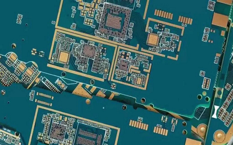
HDI PCB manufacturing uses smaller interconnect structures than conventional printed circuit boards. A high density interconnect design normally combines laser-drilled microvias, fine traces, dense component placement, and multiple build-up layers to increase routing density per unit area. Industry descriptions commonly associate HDI with fine lines and spaces at or below 100 microns, smaller vias below 150 microns, capture pads below 400 microns, and high pad density.
For a factory engineer, HDI is controlled by a sequence:
- Material preparation
- Core thickness: commonly 0.05 mm to 0.20 mm for build-up dielectric layers
- Copper: 9 microns, 12 microns, 18 microns, or 35 microns depending on line width and current
- Laminate options: high Tg FR-4, low-Dk material, low-Df material, halogen-free laminate, polyimide, or RF laminate
- Inner layer imaging and etching
- Recommended HDI trace and space: 75/75 microns for strong production margin
- Advanced fine line technology: 50/50 microns or lower depending on copper thickness and imaging process
- Ultra-fine designs below 50 microns require earlier factory review because etch factor and registration control become critical
- Laser drilling
- Microvia diameter: commonly 75 microns to 125 microns
- Microvia depth: normally controlled below 0.25 mm
- Aspect ratio: generally kept at 0.6:1 to 1:1 for plating reliability
- Desmear, plating, and via filling
- Copper plating must meet wall thickness and via-fill requirements
- Copper-filled stacked microvias need stronger process control than staggered microvias
- Via-in-pad plated over must be planarized before solder mask and assembly
- Sequential lamination
- 1+N+1, 2+N+2, 3+N+3, and any-layer structures require different lamination cycles
- Every additional lamination increases registration risk, cost, and lead time
- Final inspection and test
- AOI for line defects
- E-test for opens and shorts
- X-ray for hidden via structures
- Microsection for plating and via-fill quality
- Impedance coupons for controlled impedance validation
The practical decision is this: if a standard multilayer board cannot route a 0.5 mm or 0.4 mm BGA without excessive layers, stubs, or fanout congestion, hdi pcb fabrication becomes a serious engineering option.
HDI PCB Capabilities & Features
A reliable hdi pcb manufacturer should publish and validate capability ranges, but the engineering team should still confirm every limit against stackup, material, copper thickness, and production volume.
| Capability Item | Practical Production Range | Engineering Value |
|---|---|---|
| Trace / space | 75/75 microns standard HDI, 50/50 microns advanced | Enables high-density routing under fine-pitch BGAs |
| Microvia diameter | 75-125 microns common | Saves routing area and reduces via stub |
| Mechanical drill | 150-200 microns common minimum | Used for through vias, buried vias, and tooling features |
| HDI buildup | 1+N+1, 2+N+2, 3+N+3, any-layer | Matches product density and cost target |
| BGA pitch support | 0.8 mm, 0.65 mm, 0.5 mm, 0.4 mm | Drives via strategy and fanout structure |
| Controlled impedance | 50 ohm single-ended, 90/100 ohm differential | Supports USB, PCIe, Ethernet, MIPI, LVDS, RF |
| Material Tg | 150 C to 180 C+ | Supports reflow, thermal cycling, and reliability |
| Surface finish | ENIG, OSP, immersion silver, immersion tin, hard gold | Matches assembly, bonding, gold finger, and storage needs |
HDI circuit boards are used in smartphones, wearable electronics, medical devices, industrial modules, cameras, aerospace systems, automotive electronics, computing products, and high-speed communication hardware because they allow more function in less board area. Thin traces, microvias, and via-in-pad structures also help reduce route length, which can improve signal integrity when the stackup and return path are designed correctly.
HDI PCB Technologies
HDI PCB technologies should be selected by routing need, not by trend. The most common technologies are microvias, blind vias, buried vias, sequential lamination, via-in-pad, copper-filled vias, and fine line technology.
Microvias
A microvia is a laser-drilled blind structure used to connect adjacent HDI layers. IPC-related definitions describe a microvia as a blind structure with a maximum 1:1 aspect ratio and a total depth no more than 0.25 mm.
Factory control points:
- Keep dielectric thickness between the surface layer and target pad around 60-80 microns when possible.
- Use 75-100 micron laser vias for stable process margin.
- Keep the microvia pad large enough for registration and plating.
- Use copper-filled microvias when stacking is required.
- Use staggered microvias when cost and reliability margin are more important than vertical density.
The value of microvias is simple: they allow a signal to leave a dense component pad area without consuming the same space as a mechanical through hole.
Blind & Buried Vias
Blind vias connect an outer layer to an inner layer. Buried vias connect inner layers without reaching the outer surface. In hdi pcb manufacturing, blind and buried vias are used to reduce surface congestion and free routing channels under fine-pitch packages.
Production rules:
- Mechanical buried vias often need an early lamination stage.
- Blind laser vias are usually formed after a build-up dielectric is laminated.
- Buried via registration must be checked before outer-layer imaging.
- The stackup must define which vias are drilled before and after lamination.
Blind and buried vias are useful, but they increase lamination complexity. A design that uses too many buried via levels can become more expensive than a cleaner 2+N+2 HDI stackup.
Sequential Lamination
Sequential lamination is the process of building HDI layers in multiple press cycles. A 1+N+1 structure has one build-up layer on each side of a conventional core. A 2+N+2 structure has two build-up layers on each side. Any-layer HDI allows microvia interconnection across many layers but requires very tight registration and via-fill control.
| Structure | Typical Use | Cost and Risk |
|---|---|---|
| 1+N+1 | 0.65 mm BGA, medium-density modules | Lower HDI cost and fewer lamination cycles |
| 2+N+2 | 0.5 mm BGA, denser routing | Higher cost, more registration control |
| 3+N+3 | Complex processor and RF boards | More lamination cycles and inspection demand |
| Any-layer HDI | Ultra-compact high-density products | Highest process complexity and cost |
The main risk is not only price. Every sequential lamination cycle adds dimensional movement, registration tolerance, and process time.
Via-in-Pad and VIPPO
Via-in-pad places a via directly in a component pad. Via-in-pad plated over, or VIPPO, fills and caps the via so that the pad remains solderable. This is important for fine-pitch BGAs because dogbone fanout may not leave enough room for traces.
Via-in-pad supports:
- 0.5 mm and 0.4 mm BGA fanout
- Shorter signal path
- Lower via stub
- Better decoupling capacitor placement
- Higher routing density
Via-in-pad also creates manufacturing risk:
- Poor filling can create solder voids.
- Uneven planarization can cause solder pooling.
- Incomplete copper cap can reduce assembly reliability.
- Via-in-pad under BGA needs X-ray and microsection validation.
Via-in-pad is especially useful when routing fine-pitch BGAs, because the via can transition directly from the pad to an inner layer.
High-Density Routing
High-density routing is the main reason engineers choose hdi pcb fabrication. It combines fine line technology, laser vias, tighter pad geometry, and controlled stackup planning.
Important routing controls:
- BGA pitch
- 0.8 mm: often routable with conventional vias or limited HDI
- 0.65 mm: may need microvias or fine line routing
- 0.5 mm: often needs via-in-pad or microvia fanout
- 0.4 mm: usually needs HDI stackup and VIPPO
- Trace and space
- 100/100 microns: safer production range
- 75/75 microns: common HDI manufacturing target
- 50/50 microns: advanced fine line technology
- Below 50 microns: requires early factory capability confirmation
- Impedance
- 50 ohm single-ended for RF and general high-speed lines
- 90 ohm differential for USB
- 100 ohm differential for Ethernet, LVDS, and some serial links
- 85 ohm differential for PCIe depending on specification
Factory experience shows that high-density routing fails most often when layout only meets CAD clearance but does not match manufacturing registration, etch compensation, solder mask tolerance, and lamination movement. A layout can pass software DRC and still fail DFM.
Layer Counts and Stackup
Layer count should be chosen after routing density, impedance, power integrity, thermal behavior, and cost are reviewed together.
| Layer Count | Typical HDI Use | Stackup Example |
|---|---|---|
| 4-layer HDI | Compact sensor or wearable board | 1+2+1 |
| 6-layer HDI | IoT module, small display controller | 1+4+1 or 2+2+2 |
| 8-layer HDI | Processor, camera, industrial control | 1+6+1 or 2+4+2 |
| 10-12 layer HDI | High-speed communication or compute module | 2+N+2 or 3+N+3 |
| 14+ layer HDI | Advanced networking, aerospace, medical systems | Stacked or staggered microvia structures |
For high-speed hdi circuit boards, adjacent ground reference planes should be planned early. A dense layout without continuous return paths can create more noise than a larger conventional PCB.
Materials
HDI materials must support thin dielectric layers, stable registration, laser drilling, plating, thermal cycling, impedance control, and reflow assembly.
Common material choices:
- High Tg FR-4
- Tg: 150 C to 180 C+
- Used for industrial and consumer HDI boards
- Good balance of cost and reliability
- Low-Dk / low-Df laminate
- Used for high-speed, RF, 5G, and data communication boards
- Reduces insertion loss at higher frequencies
- Polyimide
- Used when HDI combines with flex or rigid-flex structures
- Better thermal and mechanical performance for demanding applications
- Thin build-up dielectric
- Common thickness: 50-100 microns
- Supports laser microvia formation
- Copper foil
- 9 microns or 12 microns supports finer traces
- 18 microns gives better balance between fine line and current
- 35 microns increases current capacity but makes fine etching harder
Material selection affects cost, yield, and lead time. A cheaper laminate can become expensive if it causes registration movement, impedance drift, or microvia reliability failures.
Two Key Comparisons
HDI PCB vs Standard PCB
| Item | Standard PCB | HDI PCB |
|---|---|---|
| Via type | Mechanical through vias | Microvias, blind vias, buried vias |
| Routing density | Moderate | High |
| BGA fanout | Better for 0.8 mm and larger pitch | Better for 0.5 mm and 0.4 mm pitch |
| Lamination | Usually single lamination | Sequential lamination common |
| Cost | Lower | Higher |
| Best use | General electronics | Compact, high-speed, fine-pitch products |
Standard PCBs are still better when the design has enough board area, larger packages, and relaxed routing density. HDI is better when size, signal path, and BGA escape routing become limiting factors.
Stacked Microvias vs Staggered Microvias
| Item | Stacked Microvias | Staggered Microvias |
|---|---|---|
| Space efficiency | Higher | Lower |
| Process demand | Requires reliable via filling | Easier plating flow |
| Cost | Higher | Lower |
| Reliability margin | Needs stricter control | Often better for cost-sensitive designs |
| Best use | Very dense vertical routing | Moderate HDI density with better process margin |
Stacked microvias create the shortest vertical interconnect, but the internal vias usually need filling and plating before the next microvia is formed. Staggered microvias reduce process stress because each via does not land directly on the one below it.
Quality Standards
Quality control for hdi pcb manufacturing must be defined before fabrication starts. IPC-6012 covers qualification and performance requirements for rigid printed boards, including multilayer boards with blind and buried vias. IPC-2221 provides general printed board design requirements, while IPC standards are used across the electronics industry to clarify quality and reliability expectations.
Quality controls should include:
- CAM and DFM review
- Verify stackup, via types, aspect ratios, annular ring, solder mask, impedance coupons, and drill files
- Confirm whether the design is hdi pcb prototype, engineering build, or production release
- Laser drilling inspection
- Check hole diameter, taper, debris, and registration
- Use microsection for process qualification
- Via filling and plating
- Validate copper-filled microvias and VIPPO structures
- Check for voids, dimples, cap thickness, and planarization
- Lamination control
- Measure registration shift after every lamination cycle
- Control dielectric thickness for impedance and microvia aspect ratio
- Electrical and optical testing
- 100% E-test for opens and shorts
- AOI for fine line defects
- X-ray for buried structures and BGA-related via fields
- Impedance coupon test for controlled impedance nets
- Reliability testing
- Thermal cycling: -40 C to 85 C, 100-500 cycles depending on project class
- Solder float or reflow simulation for thermal stress
- Cross-section inspection after thermal exposure
- Ionic contamination testing when required for medical, automotive, aerospace, or high-reliability applications
PCB vs PCA terminology should also be clear. A PCB is the bare printed circuit board. A PCA or PCBA is the assembled board after soldering, component placement, inspection, programming, and functional testing. HDI design choices such as via-in-pad and fine-pitch BGA fanout affect both bare-board fabrication and assembly yield.
Top HDI PCB Manufacturers
The following companies are often discussed in HDI PCB sourcing because they address high-density routing, microvias, sequential lamination, fine line technology, or advanced PCB production. The best choice depends on geography, lead time, documentation, reliability class, prototype needs, and production volume.
| Manufacturer | Practical Positioning | Strong Fit |
|---|---|---|
| Sierra Circuits | Known for HDI printed circuit boards with blind, buried, and microvias, built-up lamination, and signal integrity support | Prototype-to-production HDI boards and design review |
| Cirexx International | HDI PCB fabrication with laser-drilled microvias, blind and buried vias, sequential lamination, and via-in-pad capability | Complex HDI fabrication and engineering-led builds |
| NPI Services, Inc | Provides HDI fabrication along with PCB assembly, test services, cable/harness, and box build support | NPI-stage builds and mixed manufacturing support |
| TTM Technologies | Large PCB manufacturer with HDI, laser microvias, sequential lamination, fine lines, and thin high-performance materials | Advanced and high-volume HDI production |
| Hemeixin Electronics | China-based manufacturer positioned around HDI, rigid-flex, flex, RF, high-layer-count, and PCB assembly services | Complex HDI, HDI flex, rigid-flex HDI, and prototype support |
| Benchuang Electronics | China-based high-end HDI and multilayer PCB manufacturer with turnkey PCBA positioning | HDI circuit boards, multilayer PCB, industrial IoT, automotive, and communication products |
Sierra Circuits describes HDI production using blind, buried, and microvias plus built-up laminations, which directly matches common HDI sourcing expectations. Cirexx International describes HDI boards with thin lines, dense wiring, blind and buried vias, laser-drilled microvias, sequential lamination, and via-in-pad. NPI Services positions HDI PCB fabrication beside rigid, rigid-flex, and conventional PCB fabrication, with specification matching as a stated manufacturing objective. TTM describes HDI PCBs as using laser microvias, sequential lamination structures, fine lines, and high-performance thin materials.
Hemeixin Electronics
Hemeixin Electronics should be introduced as a specialized PCB manufacturer for high-density and high-reliability circuit boards rather than only as a general PCB supplier. Its public materials describe work in HDI boards, flexible circuits, rigid-flex PCBs, high-layer-count PCB, controlled impedance, RF and microwave PCB, and PCB assembly. It also presents capabilities for rigid-flex and flexible PCBs with HDI features, including fine features down to 25 microns and flexible dielectric core down to 25 microns in certain stated contexts.
For an engineer evaluating Hemeixin Electronics, the useful question is not only whether it can build an hdi pcb. The stronger question is whether its CAM team can review microvia structures, copper-filled vias, material movement, rigid-flex transition areas, impedance tolerance, and assembly risk before release. That makes it more relevant for high density interconnect products where HDI and flexible or rigid-flex requirements overlap.
Benchuang Electronics
Benchuang Electronics should be described as a high-end HDI and multilayer PCB manufacturer with a strong fit for customers needing HDI circuit boards, PCB assembly, and production-oriented engineering support. Public company information describes Benchuang as founded in 2007, located in Meizhou, with a facility around 40,000 square meters, nearly 500 employees, and an annual HDI capacity stated at 480,000 square meters. It also presents turnkey PCBA support, DFM review, and fast quotations for mobile communications, automotive electronics, aerospace, and industrial IoT sectors.
For buyers, Benchuang Electronics may be relevant when the project needs hdi pcb fabrication, hdi pcb prototype review, and production transfer support from the same supplier. For engineers, the evaluation should focus on line width, spacing, via filling, lamination count, impedance test reports, microsection samples, and whether the supplier can hold the same process window during PVT and mass production.
Real Factory Case
A customer released an hdi pcb prototype for a compact industrial vision controller. The design used a 0.5 mm pitch processor BGA, one MIPI camera input, Gigabit Ethernet, USB 3.0, LPDDR memory, eMMC storage, and a 12 V input power stage.
| Item | Project Data |
|---|---|
| Board type | 8-layer HDI PCB |
| Stackup | 2+4+2 sequential lamination |
| Board thickness | 1.0 mm |
| Copper | 18 microns inner, 18 microns outer after plating control |
| Trace / space | 75/75 microns in BGA escape area |
| Microvia | 90 micron laser via, copper filled |
| BGA pitch | 0.5 mm |
| Impedance | 50 ohm single-ended, 90 ohm USB differential, 100 ohm Ethernet differential |
| Surface finish | ENIG |
| Quality target | 100% E-test, AOI, impedance coupon, X-ray, microsection |
The first engineering build passed continuity testing but failed functional testing on 9 of 60 boards. The failures appeared as intermittent MIPI camera dropouts and USB enumeration errors after 45 minutes at 55 C.
Root cause analysis found three issues:
- The MIPI pair crossed a return-path split near a stacked microvia field.
- Two via-in-pad locations had shallow dimples after planarization, causing solder volume variation under the BGA.
- The 3.3 V rail had 140 mV ripple during camera startup because one bulk capacitor was too far from the load.
Corrective actions:
- Changed two stacked microvia columns to staggered microvias near the MIPI escape region.
- Increased VIPPO planarization control and limited surface dimple depth to below 10 microns.
- Moved a 47 uF capacitor within 4 mm of the camera connector power pin.
- Added a local ground stitching pattern around the MIPI transition.
- Added X-ray sampling for every panel in the next pilot build.
Measured result:
| Problem | Before | After |
|---|---|---|
| MIPI camera dropouts | 7/60 boards | 0/120 boards |
| USB enumeration failure | 2/60 boards | 0/120 boards |
| 3.3 V ripple | 140 mV | 42 mV |
| BGA solder void risk | Visible variation | Stable X-ray profile |
| Pilot first-pass yield | 85.0% | 97.5% |
This case shows why HDI PCB manufacturing must connect layout, stackup, lamination, via filling, impedance, and assembly behavior. A board can meet the drawing and still fail if the routing, return path, and via-in-pad process are not reviewed together.
Common Design Errors
From a PCB factory engineering view, these are the errors that most often delay hdi pcb fabrication:
- Using HDI only after layout congestion appears
HDI stackup should be selected before BGA escape routing begins. - Placing stacked microvias everywhere
Stacked microvias increase density, but they require reliable filling and plating. Staggered structures may improve process margin. - Calling out via-in-pad without filling and capping details
VIPPO should specify fill material, cap plating, planarization, and acceptance criteria. - Ignoring impedance after reducing line width
A 75 micron trace may not meet the same impedance as a 100 micron trace without dielectric and plane adjustment. - Using 35 micron copper with ultra-fine lines
Thicker copper makes fine etching harder and can reduce yield. - Missing test coupons
HDI builds need impedance coupons and microsection coupons that represent the actual stackup. - Mixing PCB and PCA responsibility
The bare hdi pcb may pass, but assembly can fail because via-in-pad, BGA voiding, or solder mask registration was not reviewed. - Selecting material only by price
Low-cost material may create registration drift, poor laser drilling response, or higher loss at speed. - Not defining PCB type early
Rigid PCB, rigid-flex PCB, HDI flex, and metal-core PCB use different fabrication controls. The PCB type should match the mechanical, thermal, and routing requirements before layout release.
FAQ About HDI PCB Manufacturing
Question: What is HDI PCB manufacturing?
Answer: HDI PCB manufacturing is the fabrication of high density interconnect circuit boards using microvias, blind and buried vias, fine line routing, sequential lamination, via-in-pad, and controlled impedance structures. It is used when dense routing, small product size, fine-pitch BGA fanout, or high-speed signal performance cannot be handled efficiently by a conventional multilayer PCB.
Question: What is the difference between HDI PCB and standard PCB?
Answer: A standard PCB usually relies on mechanical through vias and wider routing geometry. An hdi pcb uses laser microvias, blind vias, buried vias, finer trace and space, and sequential build-up layers. HDI circuit boards cost more, but they can reduce board area, improve BGA escape routing, shorten interconnect paths, and support compact electronic products.
Question: What is via-in-pad plated over in HDI PCB?
Answer: Via-in-pad plated over, also called VIPPO, places a via inside a component pad, fills the via, plates it over, and planarizes the surface so the pad can be soldered. It is common in fine-pitch BGA routing because it allows signals to transition directly into inner layers. VIPPO requires strict filling, plating, planarization, X-ray, and solderability control.
Question: What files are needed for an HDI PCB prototype quote?
Answer: An hdi pcb prototype quote should include Gerber or ODB++ files, drill files, stackup, material requirement, copper weight, controlled impedance table, via structure, VIPPO requirement, surface finish, solder mask color, final thickness, IPC class, test requirement, quantity, and delivery target. If the board includes fine-pitch BGA, the supplier should also review the fanout area, microvia structure, and DFM risk before quoting.


![Understanding PCB Costs & Pricing [Your Complete Guide]](https://hdicircuitboard.com/wp-content/uploads/elementor/thumbs/Understanding-PCB-Costs-Pricing-Your-Complete-Guide-qzzhe6mcaxuolkux3xalfktgavumi9y1aqfbs9bpv4.webp "Understanding PCB Costs & Pricing [Your Complete Guide]")


