
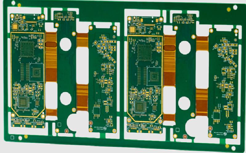
Rigid flex PCB cost is usually higher than a standard rigid PCB because it combines rigid board fabrication, flexible printed circuit materials, controlled lamination, coverlay processing, bend-area design, stiffeners, routing restrictions, and assembly validation in one structure. However, rigid flex circuit boards can reduce total system cost when they replace connectors, cables, manual wiring, secondary assembly, and field failures. For engineers, the right question is not only “How much does a rigid flex PCB cost?” but whether a PCB flex rigid design reduces the complete product cost across fabrication, assembly, test, warranty, and long-term reliability.
Rigid-Flex PCBs Typically Cost
General Estimate
A rigid flex PCB can cost roughly 2 to 5 times more than a simple rigid PCB of similar outline area, but that number can be misleading. The final price depends on layer count, flex layer count, material, copper weight, minimum line width, bend requirements, panel utilization, surface finish, tolerances, via structure, stiffener type, and production volume.
Typical cost ranges are easier to understand by build stage:
| Production Stage | Typical Quantity | Cost Behavior | Engineering Meaning |
|---|---|---|---|
| Prototype | 1-20 pieces | Highest unit cost | Setup, CAM, tooling, and process validation dominate |
| Small Batch | 25-250 pieces | Lower unit cost | Tooling spreads across more boards, but yield still matters |
| Mass Production | 500-10,000+ pieces | Lowest stable unit cost | Panelization, yield, and repeatable materials control the price |
Typical Cost Breakdown
Rigid flex PCB cost normally comes from these areas:
- Engineering and CAM review: stackup, bend radius, transition zone, drill files, impedance, coverlay, and panel layout.
- Material cost: polyimide, no-flow prepreg, adhesive or adhesiveless copper, FR-4, coverlay, stiffener, and surface finish.
- Fabrication cost: lamination, laser or mechanical drilling, plating, imaging, etching, coverlay registration, and routing.
- Tooling and setup: electrical test fixtures, forming tools, stiffener tools, punch tools, and special routing fixtures.
- Yield loss: scrap from misregistration, coverlay squeeze-out, delamination, via defects, and handling damage.
- Assembly cost: component placement, reflow profile, selective soldering, fixture support, inspection, and functional test.
Why Unit Price Changes
A prototype rigid flex PCB can look expensive because the factory still needs to build the stackup, set the lamination recipe, verify registration, check bend rules, and inspect the flex-to-rigid interface even when only a few samples are ordered. In mass production, those setup steps are spread across many units, but the design must be stable enough to hold yield.
IPC-2223 is used with IPC-2221 for flexible and rigid-flex printed board design requirements, while IPC-6013 covers qualification and performance requirements for flexible and rigid-flex printed boards. IPC-6012 covers rigid printed board qualification and performance, including multilayer boards with blind or buried vias. These standards help define design and quality language during supplier review.
Key Cost Drivers
Layer Count
Layer count is one of the strongest rigid flex PCB cost drivers. A 2-layer flexible printed circuit with two rigid stiffener zones is far cheaper than an 8-layer rigid-flex board with 2 flexible layers, buried vias, controlled impedance, and two lamination cycles.
| Build Type | Typical Structure | Cost Level | Typical Use |
|---|---|---|---|
| Simple flexible PCB | 1-2 flex layers | Low to medium | Sensor tail, LED strip, connector bridge |
| Rigid-flex basic | 2 rigid layers + 1-2 flex layers | Medium | Compact device with cable replacement |
| Multilayer rigid-flex | 4-8 rigid layers + 1-4 flex layers | High | Medical, industrial, aerospace, wearable electronics |
| HDI rigid-flex | Microvias, blind vias, sequential lamination | Very high | Dense BGA, camera module, high-speed compact system |
Cost increases because more layers require more lamination cycles, higher registration control, more inspection, and more yield risk. A design that can move from 8 layers to 6 layers often saves more than a later negotiation on unit price.
Material Choice
Material selection affects cost and reliability at the same time. Flexible areas often use polyimide films, coverlay, rolled annealed copper, electrodeposited copper, adhesive systems, or adhesiveless materials. Rigid sections often use FR-4, high-Tg FR-4, low-loss materials, or specialty laminates.
Common material choices:
- Adhesive-based flex: lower material cost, but higher Z-axis expansion and lower thermal stability than adhesiveless options.
- Adhesiveless flex: higher material cost, but better dimensional stability, bend reliability, and thermal performance.
- Rolled annealed copper: often preferred for dynamic bending due to better ductility.
- Electrodeposited copper: lower cost and common for static or flex-to-install applications.
- High-Tg FR-4: used when soldering temperature, thermal cycling, or reliability demand is higher.
- Low-Dk / low-Df material: used for high-speed or RF designs, but it raises material and processing cost.
Complexity
Complexity is not only the shape of the board. It includes the interaction of rigid zones, flexible zones, bend radius, via placement, component placement, impedance, coverlay openings, and mechanical assembly.
Rigid flex circuit boards become more expensive when they include:
- Very narrow line and space below 75/75 microns
- Small mechanical holes below 0.20 mm
- Laser microvias below 100 microns
- Controlled impedance below ±10%
- Multiple stiffener materials
- Tight bend radius below 6x to 10x flex thickness
- Dynamic bending requirement above 10,000 cycles
- Several rigid islands connected by long flex arms
- Tight outline tolerances below ±0.10 mm
- ENIG plus selective hard gold
Tooling and Setup Fees
Tooling and setup fees matter most in prototype and small-batch builds. They may include:
- CAM engineering review
- Drill tools and routing programs
- Electrical test setup
- Stiffener cutting and bonding fixture
- Forming or bending fixture
- Impedance coupons
- Cross-section coupons
- Panelization engineering
- First article inspection
For prototype builds, these costs are spread over a small quantity, so the unit cost looks high. For mass production, the setup cost becomes smaller per board, but yield and cycle time become more important.
Rigid-Flex vs Rigid PCB and Cable
Key Comparison 1
Rigid flex PCB is expensive at the bare-board level, but it can reduce total product cost when it eliminates connectors, cable harnesses, manual assembly, and field failures.
| Cost Item | Rigid PCB + Cable | Rigid Flex PCB |
|---|---|---|
| Bare board cost | Lower | Higher |
| Connector cost | Higher | Lower |
| Cable assembly | Required | Reduced or removed |
| Manual assembly | More steps | Fewer steps |
| Assembly failure risk | Higher at connectors | Lower if bend design is correct |
| Space usage | Larger | Smaller |
| Field reliability | Connector-dependent | Structure-dependent |
| Best fit | Simple product, low density | Compact, folded, high-reliability product |
When Rigid-Flex Saves Money
Rigid flex can save money when the product has:
- More than 2 board-to-board connectors
- More than 1 cable harness
- Manual wiring that takes more than 2-3 minutes per unit
- Field failures caused by connector looseness
- Space limitation that forces a smaller enclosure
- Repeated bending or vibration
- Assembly labor cost higher than bare-board cost difference
A rigid flex PCB does not always save money. It saves money when the system-level reduction in connectors, cables, rework, assembly time, and warranty risk is larger than the extra fabrication cost.
Cost-Saving Tips
Minimize Layer Count
Layer reduction is the fastest cost-saving path. Before adding layers, engineers should check:
- Can power be moved to wider traces instead of a full plane?
- Can one high-speed route be moved to a cleaner layer pair?
- Can the flex section remain 1 or 2 layers?
- Can components be moved to reduce crossings?
- Can a rigid outer-layer strategy simplify lamination?
A common factory result is that moving from 8 layers to 6 layers can reduce fabrication cost by 15% to 30%, depending on materials, stackup, and yield.
Optimize Board Size
Rigid flex panels waste material when the flex outline is long, curved, or irregular. Panel utilization below 50% can raise cost sharply because polyimide and rigid laminate are consumed even in scrap areas.
Cost-efficient layout choices:
- Keep the outline rectangular where possible.
- Avoid long unused flex tails.
- Align multiple parts for panel nesting.
- Keep stiffener shapes simple.
- Reduce unnecessary rigid island count.
- Keep fiducials, tooling holes, and coupon areas within a clean panel plan.
Use Standard Materials
Standard materials reduce lead time and sourcing risk. If the product does not require high-speed RF or dynamic bending, avoid specialty materials.
Useful default choices:
- FR-4 high Tg for rigid areas
- Polyimide flex core with 12-18 micron copper
- ENIG for fine-pitch assembly
- 25 micron or 50 micron coverlay where bend and pad access allow
- Rolled annealed copper only where dynamic bending is needed
- Adhesiveless material only where reliability justifies the cost
Avoid Tight Tolerances
Tight tolerances increase inspection and scrap. For many rigid flex PCB projects, these ranges are more production-friendly:
| Feature | Cost-Friendly Range | Higher-Cost Range |
|---|---|---|
| Trace / space | 100/100 microns | 75/75 microns or below |
| Mechanical drill | 0.25 mm and above | 0.20 mm or below |
| Outline tolerance | ±0.20 mm | ±0.10 mm or tighter |
| Impedance tolerance | ±10% | ±5% |
| Flex bend radius | 10x flex thickness or higher | 6x flex thickness or lower |
| Coverlay registration | 0.20 mm clearance | Below 0.10 mm clearance |
Consider Semi-Flex
Semi-flex can reduce cost when the bend is only used during installation and the board will not bend repeatedly in the field. It is not a substitute for dynamic flexible PCB applications. It may fit products where the board bends once into an enclosure and then remains fixed.
How to Reduce Rigid-Flex PCB Cost
Design Simplification
Design simplification reduces both fabrication cost and assembly risk. The goal is to remove unnecessary complexity before layout release.
Strong simplification methods:
- Use rigid flex only where it eliminates real connectors or wiring.
- Keep flex arms straight and short.
- Avoid unnecessary rigid islands.
- Move heavy components away from flex transitions.
- Keep components out of bend zones.
- Avoid overlapping traces on opposite flex layers in dynamic areas.
- Use the same stiffener thickness where possible.
- Reduce unique material combinations.
Reduce Layer Count
A PCB flex rigid design should not automatically copy the layer count of a rigid PCB. The flex region may not need all rigid section layers.
Cost-saving layer strategies:
- Use 6 rigid layers with 2 flex layers instead of 8 continuous layers.
- Keep ground return in the rigid area and use controlled flex routing only where needed.
- Avoid carrying power planes through the flex section unless required.
- Use local decoupling near rigid component zones instead of wide flex power copper.
- Use cross-hatching for ground in flex areas when impedance and EMI allow it.
Minimize Flexible Areas
Flexible area is expensive because it uses polyimide, coverlay, careful lamination, and special handling. A larger flex section also increases risk of tearing, creasing, and panel waste.
Factory rules:
- Keep flex length only as long as the bend geometry needs.
- Keep the flex section width stable.
- Avoid sharp reentrant corners.
- Use corner radius above 1.0 mm, preferably 1.5 mm or larger.
- Add strain relief at the rigid-to-flex interface.
- Do not place holes in bend areas.
Use Rigid Outer Layers
Using rigid outer layers can reduce complexity in some structures because components, solder mask, and assembly features stay on stable rigid surfaces. This helps avoid expensive component placement or soldering on flexible material.
Benefits:
- Better SMT stability
- Easier solder paste printing
- More stable component coplanarity
- Lower assembly scrap
- Cleaner inspection
- Reduced need for local stiffeners
Material and Fabrication Choices
Standardize Materials
Material standardization lowers purchasing cost and reduces variation. A flex rigid PCB manufacturer can quote faster when the material stack is familiar.
Recommended standardization:
- Use one flex core thickness across the product family.
- Use one coverlay thickness where possible.
- Use one copper weight unless current or impedance requires change.
- Use ENIG consistently for fine-pitch assembly.
- Avoid mixing multiple stiffener materials in one board unless needed.
- Lock material suppliers before DVT or PVT.
Use Proper Copper Weights
Copper weight affects cost, etching, flexibility, current capacity, and bend reliability.
| Copper Choice | Best Use | Cost Impact |
|---|---|---|
| 9 micron copper | Fine line flex routing | Higher process control |
| 12 micron copper | Fine flexible printed circuit designs | Good for compact routing |
| 18 micron copper | Balanced routing and current | Common practical choice |
| 35 micron copper | Power and current capacity | Harder fine-line etching |
| 70 micron copper | High current zones | Not ideal for tight flex bends |
Using thicker copper everywhere is a common mistake. It increases etch difficulty and reduces flexibility. A better approach is to use thicker copper only where current requires it.
Avoid Small Holes and Tight Tolerances
Small holes increase drill cost, plating risk, and inspection demand.
Cost-friendly choices:
- Use 0.25 mm or larger mechanical vias when possible.
- Avoid laser vias unless HDI density requires them.
- Keep annular ring above 0.15 mm where possible.
- Avoid blind and buried vias unless routing demands them.
- Avoid slots below 0.60 mm unless the supplier confirms routing capability.
Adhesiveless Materials
Adhesiveless materials cost more than adhesive-based flex laminates, but they can reduce reliability risk in high-temperature, high-bend, or fine-line applications. They are useful when the product needs dynamic bending, high layer stability, or strong dimensional control.
Use adhesiveless materials when:
- Dynamic bending is required
- Bend radius is tight
- Fine-line routing is used
- High temperature cycling is expected
- The product is medical, aerospace, automotive, or high-reliability industrial hardware
Layout Optimization
Panelization Efficiency
Panelization affects rigid flex PCB cost more than many engineers expect. A design with poor nesting can waste expensive flex material and reduce factory yield.
Factory targets:
- Panel utilization above 65% is generally better.
- Below 50% utilization can create a visible cost increase.
- Keep flex tails aligned in the same direction where possible.
- Avoid shapes that require large empty spaces between parts.
- Keep break-off tabs away from flex sections.
- Add coupons without breaking the main nesting plan.
Use Cross-Hatching
Cross-hatching copper in flex areas can improve flexibility and reduce stress compared with solid copper. It is often used for shielding or ground reference where a full solid plane would make the flex section too stiff.
Typical cross-hatch choices:
- 30% to 60% copper coverage
- 45-degree hatch angle
- Rounded hatch intersections
- No sharp copper corners in the bend area
- Full copper avoided across repeated bend zones
Cross-hatching should not be used blindly on controlled impedance traces. If impedance is required, the stackup and field solver must include the hatch geometry.
Round Corners
Sharp inside corners create tear points. Rounded corners reduce stress concentration and improve handling yield.
Recommended practices:
- Use outside radius above 1.0 mm
- Use inside radius above 1.5 mm where space allows
- Add relief holes above 1.0 mm at slit ends
- Avoid narrow slots ending in sharp corners
- Keep copper away from flex outline edges by 0.25 mm or more when possible
Manufacturing Considerations
Early CM Engagement
Early CM engagement means the flex rigid PCB manufacturer reviews the design before layout is fully locked. This reduces costly redesign after CAM.
The review should include:
- Layer count and flex layer count
- Bend radius and bend direction
- Rigid-to-flex transition zone
- Coverlay opening and pad capture
- Stiffener material and thickness
- Copper weight and trace width
- Drill sizes and annular ring
- Impedance stackup
- Panelization
- Test coupon and inspection plan
Use Standardized Components
Standardized components reduce assembly and procurement cost. Rigid flex boards often cost more when the design uses rare connectors, non-standard stiffeners, custom adhesives, or components with unstable supply.
Component choices that help cost:
- Common FPC connectors
- Standard board-to-board connectors
- Standard screw sizes
- Standard stiffener thickness
- Standard SMT package sizes
- Common passive values
- Avoiding unnecessary 0201 parts unless space requires them
Quality Control
Quality control for rigid flex circuit boards must cover both rigid and flexible behavior.
Quality control checklist:
- IPC-2221 design review for generic board requirements
- IPC-2223 review for flex and rigid-flex design requirements
- IPC-6012 review for rigid section qualification and performance
- IPC-6013 review for flexible and rigid-flex board qualification and performance
- AOI for fine-line defects
- 100% electrical test for opens and shorts
- Cross-section for plating and lamination quality
- Peel strength validation where required
- Bend test for flex areas
- Impedance coupon test for controlled lines
- Visual inspection for coverlay registration and adhesive squeeze-out
- Final outline and stiffener position inspection
Real Factory Case
Project Background
A handheld industrial scanner used two rigid PCBs, one flexible cable, two board-to-board connectors, and one small daughterboard for a side button module. The customer wanted to reduce connector failures and shorten assembly time. The original assembly had a 3.2% field return rate related to connector looseness after drop and vibration.
The redesigned structure used a rigid flex PCB.
| Item | Original Design | Rigid Flex Redesign |
|---|---|---|
| Board structure | 2 rigid PCBs + 1 cable | 6-layer rigid-flex PCB |
| Flex layers | External cable | 2 internal flex layers |
| Rigid layers | 4 + 2 layers | 6 rigid layers |
| Total connectors | 4 connectors | 1 service connector |
| Assembly time | 6.5 minutes/unit | 3.1 minutes/unit |
| Board thickness | 1.0 mm rigid sections | 1.0 mm rigid, 0.12 mm flex |
| Trace / space | 100/100 microns | 100/100 microns, 75/75 local |
| Finish | ENIG | ENIG |
| Bend radius | Cable bend uncontrolled | 5.0 mm controlled bend |
Problem Found
The first prototype build had three cost and reliability issues:
- Flex tail too long caused poor panel utilization at 48%.
- The design used 35 micron copper through the flex section, making the bend too stiff.
- Two stiffeners had different thicknesses, requiring extra bonding setup.
Corrective Action
The factory review changed the design:
- Flex length reduced by 12 mm
- Panel utilization improved from 48% to 68%
- Flex copper changed from 35 microns to 18 microns
- Stiffener thickness standardized at 0.20 mm
- Inside corners changed from sharp corners to 1.5 mm radius
- Bend area copper changed to cross-hatch ground
- Component placement moved 3.0 mm away from the rigid-to-flex transition
Measured Result
| Metric | Before Redesign | After Redesign |
|---|---|---|
| Connector count | 4 | 1 |
| Assembly time | 6.5 min/unit | 3.1 min/unit |
| Panel utilization | 48% | 68% |
| Prototype scrap | 14.0% | 4.5% |
| Field connector return | 3.2% | 0.4% |
| Estimated total system cost | Baseline | 11.8% lower |
The bare rigid flex PCB cost was higher than the previous rigid boards, but total product cost decreased because connectors, cable assembly, manual labor, rework, and field returns were reduced.
Common Design Errors
Cost Errors from Layout
- Carrying all rigid layers through the flex section
- Adding blind vias without routing need
- Using 35 micron copper in dynamic bend areas
- Placing components too close to the flex transition
- Using irregular outlines that waste panel area
- Setting unnecessary ±0.05 mm outline tolerance
- Adding coverlay openings with too little clearance
Cost Errors from Materials
- Using adhesiveless material for static applications without reliability need
- Selecting low-loss material for non-high-speed layers
- Mixing too many copper weights in one stackup
- Using non-standard stiffener thickness
- Changing materials after prototype approval
- Selecting surface finish without assembly need
Cost Errors from Manufacturing
- Engaging the manufacturer after layout completion
- Not defining bend direction and bend radius
- Missing impedance coupons
- Missing flex test requirements
- Confusing PCB and PCA cost
- Ignoring assembly labor in the cost comparison
- Not asking for panelization feedback before quote
PCB means the bare printed circuit board. PCA means the assembled circuit board with components, solder joints, labels, firmware, inspection records, and functional test results. A rigid flex PCB may cost more as a bare PCB, but the PCA can cost less when connectors and cable assembly are removed.
FAQ About Rigid Flex PCB Cost
Question: Why does rigid flex PCB cost more than rigid PCB?
Answer: Rigid flex PCB costs more because it uses flexible printed circuit materials, rigid laminate, coverlay, controlled lamination, stiffeners, special routing, and more inspection. It also requires careful review of bend radius, transition zones, copper weight, and panelization. The cost is higher at bare-board level, but the total system cost can be lower when connectors, cables, manual assembly, and field failures are reduced.
Question: How can engineers reduce rigid flex PCB cost?
Answer: Engineers can reduce rigid flex PCB cost by minimizing layer count, keeping flex areas short, using standard materials, avoiding tight tolerances, reducing small holes, improving panel utilization, standardizing stiffeners, using cross-hatched copper in bend areas, and engaging the manufacturer before layout release. The most effective savings often come from removing unnecessary layers and improving panel utilization.
Question: When does rigid flex save money?
Answer: Rigid flex saves money when it replaces multiple connectors, cable harnesses, manual soldering, secondary assembly, and failure-prone interconnects. A design with two or more board-to-board connectors, repeated vibration, tight packaging, or field connector failures may justify rigid flex even when the bare PCB price is higher.


![Understanding PCB Costs & Pricing [Your Complete Guide]](https://hdicircuitboard.com/wp-content/uploads/elementor/thumbs/Understanding-PCB-Costs-Pricing-Your-Complete-Guide-qzzhe6mcaxuolkux3xalfktgavumi9y1aqfbs9bpv4.webp "Understanding PCB Costs & Pricing [Your Complete Guide]")


