
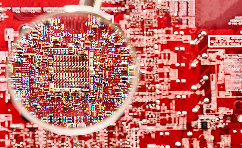
An HDI PCB DFM checklist is a manufacturing review document used to confirm whether a high density interconnect board can be fabricated with stable yield before the design is released. A reliable DFM review checks microvia aspect ratio, annular rings, via structures, via-in-pad processing, trace width and spacing, drill-to-copper clearance, copper pours, stackup symmetry, dielectric materials, solder mask openings, surface finish, silkscreen readability, LDI imaging, laser drilling, cost control, and quality inspection. For engineers, the purpose is not only to pass CAD rules. The purpose is to make sure the hdi pcb manufacturer can build the board repeatedly from prototype to production without hidden plating, registration, solderability, impedance, or assembly defects.
Via and Drill Specifications
Microvia Aspect Ratio
| Via Depth | Via Diameter | Aspect Ratio | DFM Judgment |
|---|---|---|---|
| 50 microns | 100 microns | 0.50:1 | Strong margin |
| 60 microns | 90 microns | 0.67:1 | Stable production range |
| 75 microns | 100 microns | 0.75:1 | Reliable HDI target |
| 80 microns | 80 microns | 1.00:1 | Upper boundary |
| 90 microns | 75 microns | 1.20:1 | High risk for standard microvia |
Microvia aspect ratio is one of the first items in any HDI PCB DFM checklist. It is calculated as via depth divided by via diameter. For laser microvias, a 1:1 ratio is usually treated as the upper boundary, while 0.75:1 or lower gives better plating margin in production.
A microvia that looks acceptable in CAD can fail in plating if the dielectric thickness changes after lamination. The stackup and microvia rule must be locked together before final routing.
Annular Rings
| Item | Conservative Target | Dense HDI Target |
|---|---|---|
| Microvia annular ring | 75 microns | 50 microns by review |
| Capture pad oversize | Via diameter + 100-150 microns | Via diameter + 75-100 microns |
| Mechanical via annular ring | 100 microns or more | 75 microns by review |
| Plane clearance | 200-300 microns | 150-250 microns by review |
Annular ring controls the copper land remaining around a via after drilling or laser registration tolerance. In HDI boards, small pads and thin dielectrics make this tolerance more sensitive than in conventional multilayer boards.
Practical DFM checks:
- Laser microvia landing pad should usually be 200-300 microns.
- Dense HDI designs may use smaller pads after manufacturer approval.
- Mechanical buried via pads need larger tolerance than laser microvias.
- Target pads must allow lamination movement.
- Via-to-plane clearance must match voltage, process, and registration limits.
Via Structures
| Via Structure | Best Use | DFM Risk |
|---|---|---|
| Through via | General routing and power | Routing blockage and stub length |
| Blind microvia | BGA breakout and short transitions | Plating and landing alignment |
| Buried via | Internal layer routing | Extra core processing |
| Staggered microvia | Reliable multi-layer HDI routing | Uses more lateral area |
| Stacked microvia | Maximum vertical density | Needs copper fill and X-ray |
| Via-in-pad | Fine-pitch BGA and QFN pads | Requires fill, cap, and planarization |
Via structure selection affects cost, yield, and reliability. A high density interconnect board may use through vias, blind vias, buried vias, staggered microvias, stacked microvias, or via-in-pad structures.
Stacked vias save routing area but add process risk. Staggered vias are usually more cost-effective when the layout has enough space.
Via-in-Pad Process
Via-in-Pad VIP
Via-in-Pad, also called VIP, places a via directly inside a component solder pad. It is used in fine-pitch BGA, QFN thermal pads, processor fanout, memory fanout, RF grounding, and compact power designs.
VIP should be checked when:
- BGA pitch is 0.5 mm or smaller.
- Dogbone fanout cannot fit.
- Decoupling loops must be shortened.
- Thermal transfer is needed under an exposed pad.
- High-speed signals need direct layer access.
- Board outline cannot increase.
Open vias inside solder pads should not be used for normal SMT assembly because solder can wick into the via and reduce solder joint volume.
Via Fill Types
| Fill Type | Best Use | Key DFM Control |
|---|---|---|
| Nonconductive epoxy fill | General VIPPO and BGA pads | Prevents solder wicking |
| Conductive fill | Ground or thermal transfer | Controls conductivity and expansion |
| Copper fill | Stacked microvias and high-reliability HDI | Improves vertical interconnect strength |
| Resin plug with copper cap | Standard solderable via-in-pad | Needs planarization |
| Open via | Non-solderable areas only | Not suitable for solder pads |
Via fill type must match the reason for using the via. The cheapest fill is not always the best manufacturing choice.
VIPPO Requirements
VIPPO means via-in-pad plated over. The via is drilled, plated, filled, capped, and planarized to create a flat solderable pad.
Required DFM callouts:
- Via fill material
- Copper cap requirement
- Maximum dimple after planarization
- Surface finish
- X-ray inspection for filled VIP areas
- Microsection coupon near critical VIP fields
- BGA or QFN assembly validation
For fine-pitch BGA, a dimple above 10-15 microns can create uneven solder collapse.
Trace, Space and Clearance
Trace Width and Spacing
| Routing Class | Trace / Space | Copper Thickness | Common Use |
|---|---|---|---|
| Standard multilayer | 100/100 microns | 18-35 microns | General routing |
| Standard HDI | 75/75 microns | 12-18 microns | Dense digital routing |
| Fine BGA breakout | 50/50 microns | 9-12 microns | 0.4 mm to 0.5 mm BGA |
| Advanced local HDI | Below 50/50 microns by qualification | 5-9 microns | Special high-density zones |
Trace width and spacing must match copper thickness, imaging method, etching margin, and finished impedance target. HDI PCB fabrication often uses thinner copper on fine-line layers because thick copper is harder to etch accurately.
Fine trace rules should be applied only where needed. Using 50/50 micron routing across the whole board increases cost, lowers yield, and makes panel compensation harder.
Drill-to-Copper
Drill-to-copper clearance prevents shorts caused by drill wander, lamination shift, laser registration error, or copper movement. In HDI designs, this clearance must be reviewed separately for laser microvias, mechanical buried vias, and through vias.
Practical checks:
- Keep through via drill-to-copper clearance larger than laser microvia clearance.
- Confirm inner-layer clearance after lamination scaling.
- Check clearance near BGA escape channels.
- Review copper-to-board-edge clearance.
- Keep high-voltage nets outside dense clearance assumptions.
- Confirm whether the manufacturer measures finished hole or tool size.
Copper Pours
Copper pours affect plating balance, etching uniformity, impedance, and warpage. In HDI PCB DFM, copper should be balanced across layers and across panel zones.
Copper pour checks:
- Avoid large isolated copper islands.
- Keep copper density balanced between opposite layers.
- Use thieving copper if the fabricator requires it.
- Avoid sharp copper neck-downs near microvias.
- Do not place copper pours under high-speed traces without reference control.
- Keep copper clear from flex or rigid-flex bending areas when applicable.
- Confirm copper pour connection style for thermal pads.
Stackup and Materials
Stackup Symmetry
| Stackup Item | DFM Requirement | Manufacturing Reason |
|---|---|---|
| Layer symmetry | Copper and dielectric balanced around center | Controls warpage |
| Build-up layers | Same count on both sides when possible | Improves lamination stability |
| Copper balance | Similar copper density on paired layers | Reduces bow and twist |
| Core thickness | Stable and available material | Improves repeatability |
| Lamination cycle | Minimized where possible | Reduces cost and registration risk |
Stackup symmetry reduces warpage and improves lamination stability. HDI boards often go through multiple lamination cycles, so asymmetry can create bow, twist, registration drift, or soldering problems.
A 2+6+2 stackup is often more stable than an unbalanced build-up structure if routing permits it.
Dielectric Materials
| Material Type | Typical Use | DFM Concern |
|---|---|---|
| High-Tg FR-4 | Industrial HDI boards | Stable supply and cost control |
| Low-loss laminate | PCIe, RF, high-speed digital | Dk, Df, copper roughness |
| Thin build-up dielectric | Laser microvia layers | Aspect ratio and registration |
| Halogen-free laminate | Environmental requirement | Availability and lamination behavior |
| Polyimide | Rigid-flex HDI | Moisture and process control |
Material choice affects impedance, microvia depth, thermal behavior, soldering reliability, and lead time.
Common DFM material checks:
- Confirm high-Tg FR-4 or low-loss laminate availability.
- Use low Dk and low Df materials only where signal speed requires them.
- Confirm pressed dielectric thickness, not only nominal prepreg thickness.
- Keep build-up dielectric within the microvia aspect ratio limit.
- Confirm CAF resistance for high-voltage or humid environments.
- Match material family across sequential lamination cycles when possible.
Controlled Impedance
Impedance should be reviewed with the stackup. A Gerber file alone cannot define impedance.
Required data:
- Target impedance, such as 50 ohm, 85 ohm, 90 ohm, or 100 ohm
- Tolerance, such as +/-10% or +/-5%
- Routing layer
- Reference plane
- Dielectric thickness
- Copper thickness
- Solder mask condition
- Test coupon structure
- TDR test requirement
Solder Mask and Surface Finish
Surface Finishes
| Surface Finish | Best Use | DFM Concern |
|---|---|---|
| ENIG | Fine-pitch BGA and general HDI | Flat pads and stable solderability |
| ENEPIG | Wire bonding and high-reliability assembly | Higher cost |
| OSP | Cost-sensitive SMT | Shelf life and handling |
| Immersion silver | High-speed and RF applications | Tarnish and packaging control |
| Immersion tin | Press-fit and selected applications | Whisker and handling review |
| HASL | Low-cost conventional boards | Not ideal for fine-pitch HDI |
Surface finish affects solderability, pad flatness, bonding method, shelf life, cost, and fine-pitch assembly yield.
For via-in-pad and fine-pitch BGA, ENIG or ENEPIG is usually easier to control than HASL because pad flatness matters.
Solder Mask Expansion
Solder mask expansion controls mask clearance around pads. If expansion is too small, mask can cover part of the pad. If it is too large, solder bridges may increase in fine-pitch areas.
Practical values:
- General SMT pad expansion: 50-75 microns by process.
- Fine-pitch BGA expansion: reviewed by pitch and solder mask registration.
- Solder mask dam between pads: confirmed by actual mask capability.
- Via tenting: used only where solderability is not affected.
- VIP areas: mask opening must match pad and fill/cap strategy.
Mask Openings
Mask openings should be checked for BGA pads, QFN thermal pads, test pads, exposed copper, and via-in-pad regions.
DFM checks:
- Confirm solder mask defined or copper defined pads.
- Avoid narrow solder mask dams below process capability.
- Keep mask openings away from filled via defects.
- Confirm mask clearance around castellated edges if used.
- Avoid silkscreen over exposed copper or pads.
Silkscreen and Assembly
Text Legibility
| Silkscreen Item | Practical Target | Reason |
|---|---|---|
| Text height | 0.8-1.0 mm minimum | Readability |
| Line width | 0.10-0.15 mm minimum | Print stability |
| Clearance to pad | 0.15-0.20 mm minimum | Avoid contamination |
| Polarity mark | Required for diodes, LEDs, ICs | Assembly verification |
| Pin 1 mark | Required for ICs and connectors | Orientation control |
Silkscreen is still part of DFM because unreadable text slows inspection and repair. Dense HDI boards often have limited surface area, but reference designators still need to be useful.
Component Markings
Component markings should support assembly, inspection, and field service.
Required checks:
- IC pin 1 orientation visible.
- Connector polarity marked.
- LED polarity marked.
- Test points named.
- Programming connector labeled.
- High-voltage areas marked.
- Revision and date code included if required.
- Barcode or QR traceability area reserved.
Assembly Data
An HDI PCB prototype should include assembly files before the first build.
Required manufacturing files:
- Gerber or ODB++ data
- NC drill files
- Laser drill files
- IPC-356 netlist when available
- Stackup drawing
- Fabrication drawing
- Assembly drawing
- BOM
- Pick-and-place file
- Test point list
- Impedance table
- Via fill and cap notes
- Surface finish requirement
LDI, Contact Imagery and Laser Drill Technology
LDI and Contact Imagery
| Imaging Method | Best Use | DFM Effect |
|---|---|---|
| Contact imagery | Standard trace and space | Lower cost for wider features |
| LDI | Fine HDI trace and space | Better registration and fine-line yield |
| Advanced LDI | Sub-50 micron local features | Higher cost, tighter process control |
LDI means laser direct imaging. It exposes the photoresist directly from digital data and is often preferred for fine-line HDI because it improves registration and removes film-related distortion. Contact imagery can still be used for less demanding designs, but dense HDI usually benefits from LDI.
Laser Drill Technology
Laser drilling is used for microvias and fine HDI layer transitions. The process must control hole diameter, taper, residue, target pad condition, and plating quality.
Laser drill checks:
- Confirm laser via diameter.
- Confirm dielectric thickness and aspect ratio.
- Confirm target pad size.
- Check for glass weave or resin variation.
- Verify desmear and debris removal.
- Use microsection for critical via fields.
- Use X-ray for stacked or filled vias.
Building Non-Conventional HDI Circuit Boards
When Non-Conventional HDI Is Needed
Non-conventional HDI circuit boards include any-layer HDI, cavity boards, rigid-flex HDI, mixed material HDI, embedded components, semi-additive process boards, and ultra-fine feature boards.
Use non-conventional structures when:
- BGA pitch is below standard breakout limits.
- The board must fit into a very thin enclosure.
- High-speed routing requires very short transitions.
- Rigid-flex integration removes connectors.
- RF, power, and digital sections require different materials.
- Standard subtractive etching cannot hold the required trace width.
Manufacturing Risk Control
Non-conventional HDI boards need early fabricator review. The risk is rarely one feature alone. It is usually the interaction between material, copper, lamination, laser drilling, imaging, plating, and inspection.
Required controls:
- Process flow approved before layout release.
- Stackup locked before routing.
- Material availability confirmed.
- Design rules separated by zone.
- Test coupons placed near critical features.
- Pilot build data reviewed before volume release.
- Assembly defects fed back into PCB process review.
Cost-Effective HDI PCBs
Cost Drivers
| Cost Driver | Higher-Cost Choice | Cost-Control Choice |
|---|---|---|
| Stackup | Any-layer HDI | 1+N+1 or 2+N+2 if routing allows |
| Microvias | Stacked everywhere | Staggered where space allows |
| Trace width | 50/50 microns full board | Local fine lines only |
| Material | Low-loss laminate on every layer | Low-loss only on critical layers |
| VIP | Via-in-pad on all pads | VIP only under dense BGA or thermal pads |
| Inspection | No plan until failure | Risk-based QC defined before build |
Cost-effective HDI PCBs are not made by removing important quality controls. They are made by using advanced features only where they solve a real design problem.
Practical Cost Controls
Use these engineering controls:
- Keep the HDI region local where possible.
- Avoid stacked microvias unless density requires them.
- Use standard material when signal speed allows it.
- Keep copper thickness compatible with fine traces.
- Use 75/75 micron routing outside dense package areas.
- Choose ENIG instead of more expensive finishes unless the assembly requires them.
- Confirm panel utilization before final outline.
- Complete DFM before ordering an expedited hdi pcb prototype.
HDI PCB Benefits
Engineering Benefits
HDI PCB benefits appear when the board uses advanced features for a clear engineering reason.
Main benefits:
- Smaller board outline
- Better BGA fanout
- Shorter signal paths
- Lower through-via blockage
- Improved routing density
- More room for decoupling capacitors
- Better high-speed transition control
- Lighter product assembly
- Fewer connectors in compact designs
Manufacturing Benefits
From a manufacturing view, HDI can improve the whole product when it reduces layer count, lowers assembly complexity, eliminates daughterboards, or improves signal margin.
HDI is valuable when it reduces system-level risk, not only when it makes a board smaller.
Real Factory Case
Project Background
| Item | First Release | DFM Revision |
|---|---|---|
| Board type | HDI PCB | HDI PCB |
| Layer count | 10 layers | 10 layers |
| Stackup | 2+6+2 | 2+6+2 adjusted |
| BGA pitch | 0.4 mm | 0.4 mm |
| Fine trace area | Full board | BGA and high-speed zones only |
| Trace / space | 50/50 microns full board | 50/50 local, 75/75 general |
| Microvia | Stacked and staggered mixed | Staggered except critical BGA escapes |
| Surface finish | ENIG | ENIG |
| Inspection | AOI and E-test | AOI, E-test, X-ray, microsection, TDR |
A compact AI camera board used a 0.4 mm BGA processor, LPDDR memory, MIPI camera input, USB 3.0, PMIC, flash, and two board-to-board connectors. The original design used a 10-layer HDI stackup with 50/50 micron routing across the full board and stacked microvias in several non-critical regions.
Problem Found
The first build passed bare-board electrical test, but pilot assembly found several issues:
- 6 of 100 boards showed BGA void concentration above the internal limit.
- 4 boards had intermittent MIPI dropout after 60 C thermal soak.
- 3 panels showed marginal stacked microvia filling in X-ray review.
- Finished trace width variation reached 12 microns in wide copper imbalance areas.
- First-pass functional yield was 89.0%.
Factory review found the main causes:
- 50/50 micron routing was used outside the actual dense region.
- Stacked microvias were used where staggered vias would fit.
- VIPPO dimple limit was not clearly defined.
- One impedance coupon did not match the real routing layer.
- Copper density imbalance affected etching uniformity.
- The solder mask opening around one QFN thermal pad increased voiding.
Corrective Result
| Metric | First Release | DFM Revision |
|---|---|---|
| BGA void-related rejects | 6/100 | 1/220 |
| MIPI thermal-dropout failures | 4/100 | 0/220 |
| Marginal stacked via findings | 3 panels | 0 panels |
| Finished trace width variation | 12 microns | 5 microns |
| First-pass functional yield | 89.0% | 98.4% |
| Estimated fabrication cost | Baseline 100% | 82% of baseline |
The DFM revision changed the design rules without increasing board size:
- Localized 50/50 micron routing under the BGA only.
- Changed three stacked microvia areas to staggered microvias.
- Added VIPPO dimple limit below 10 microns.
- Added X-ray for critical filled via fields.
- Added microsection coupons near the BGA fanout.
- Rebuilt impedance coupons to match real routing layers.
- Adjusted copper pour density around high-speed regions.
- Changed QFN thermal mask opening to reduce solder voiding.
The improvement came from simplifying HDI only where it was not needed while tightening quality control where the design was truly dense.
Common HDI DFM Errors
Via and Drill Errors
- Microvia aspect ratio above the stable process window.
- Missing laser drill file.
- No via structure map.
- Stacked vias used without copper fill.
- Via-in-pad used without fill and cap notes.
- Annular ring too small for lamination movement.
- Mechanical drill-to-copper clearance too tight.
Trace and Stackup Errors
- Routing 50/50 micron traces across the full board.
- Thick copper used in fine-line areas.
- Stackup changed after impedance routing.
- Dielectric thickness not confirmed after pressing.
- Unbalanced copper pours causing warpage.
- No impedance coupon for high-speed nets.
Assembly and Documentation Errors
- Silkscreen placed over pads.
- Missing pin 1 marks.
- Solder mask openings too large for fine pitch.
- No BGA X-ray requirement.
- No IPC class on fabrication drawing.
- No surface finish requirement.
- No BOM, pick-and-place, or assembly drawing for prototype build.
FAQ
Question: What is an HDI PCB DFM checklist?
Answer: An HDI PCB DFM checklist is a manufacturing review list used to verify microvias, drill rules, annular rings, via structures, trace width, clearance, stackup, materials, solder mask, surface finish, silkscreen, and inspection requirements before fabrication.
Question: What microvia aspect ratio is best for HDI PCB fabrication?
Answer: A microvia aspect ratio at or below 1:1 is the common upper limit, while 0.75:1 or lower gives better plating margin. The final value depends on via diameter, dielectric thickness, material, plating process, and reliability class.
Question: How can engineers reduce HDI PCB cost without reducing reliability?
Answer: Engineers can reduce cost by localizing fine-line routing, avoiding unnecessary stacked microvias, choosing standard materials where possible, using staggered vias when space allows, confirming panel utilization, and completing DFM before prototype release.
Question: Why is via-in-pad risky in HDI PCB assembly?
Answer: Via-in-pad is risky when the via is not filled, capped, and planarized. Open vias inside solder pads can wick solder during reflow, causing BGA voids, weak joints, poor collapse, and hidden assembly failures.


