







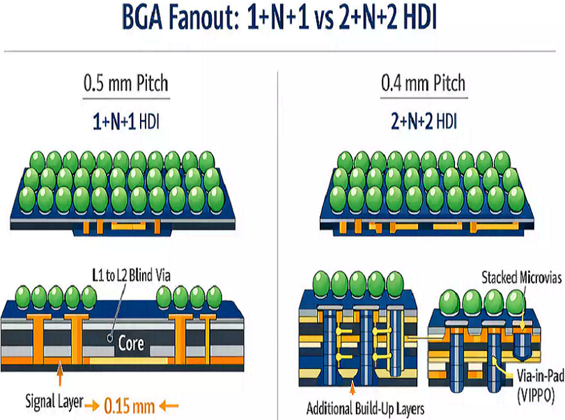
Selecting the right High-Density Interconnect (HDI) PCB supplier is critical for electronic products that require compact design, high-speed performance, and long-term reliability. A qualified HDI PCB manufacturer must provide more than basic PCB production capability. Engineers should evaluate microvia precision, sequential lamination technology, fine-line fabrication, impedance control, testing capability, engineering support, certification compliance, and supply chain stability.
The right supplier should demonstrate proven HDI PCB fabrication experience with structures such as 1+N+1, 2+N+2, and 3+N+3, support line width and spacing down to 3/3 mil, manufacture reliable microvias from 75μm to 150μm, and provide inspection data based on standards such as IPC-2221, IPC-6012, IPC-A-600, and IPC-A-610. A strong HDI PCB supplier helps customers reduce manufacturing risks, shorten prototype cycles, and achieve stable production performance for applications including medical devices, aerospace, automotive electronics, and high-speed computing systems.
Understanding HDI PCB Supplier Requirements
Why HDI PCB Capability Matters
HDI PCB technology enables engineers to integrate more functions into smaller electronic devices by using advanced interconnect structures.
Compared with conventional multilayer PCBs, HDI circuit boards use:
- Laser-drilled microvias
- Blind vias
- Buried vias
- Via-in-Pad plated over (VIPPO)
- Sequential lamination
- Fine-line routing
These technologies improve:
- Signal integrity
- Component density
- Power distribution
- Product miniaturization
- High-frequency performance
A supplier without advanced HDI PCB fabrication capability may produce boards that pass basic electrical tests but fail during assembly, thermal cycling, or field operation.
Key HDI Manufacturing Capabilities
A professional HDI PCB manufacturer should demonstrate capability in:
- Laser drilling
- Microvia filling
- Copper electroplating
- Sequential lamination
- Fine-line imaging
- Controlled impedance manufacturing
- Automated optical inspection
- Reliability testing
Typical advanced HDI PCB production requirements include:
| Manufacturing Parameter | Typical HDI Capability |
|---|---|
| HDI Structure | 1+N+1, 2+N+2, 3+N+3 |
| Microvia Diameter | 75μm-150μm |
| Line Width and Spacing | 3/3 mil-5/5 mil |
| Board Thickness | 0.8mm-2.0mm |
| Layer Count | 6-20 layers |
| Impedance Control | 50Ω ±10%, 90Ω/100Ω differential |
Verify Advanced Manufacturing Capabilities
Microvia Precision
Microvia quality is one of the most important indicators when selecting an HDI PCB supplier.
Microvias are typically created using laser drilling instead of mechanical drilling. The process requires precise control of:
- Laser energy
- Hole diameter
- Copper plating thickness
- Resin filling
- Alignment accuracy
Common microvia specifications:
- Diameter: 75μm-150μm
- Aspect ratio: approximately 0.75:1 or lower
- Copper thickness: typically 15μm-25μm
- Layer-to-layer registration: within ±50μm for advanced HDI
Poor microvia manufacturing may cause:
- Bottom microvia cracks
- Copper separation
- Open circuits after thermal cycling
- Reliability failures during product lifetime
Sequential Lamination
Sequential lamination is a core HDI PCB fabrication process.
Unlike traditional multilayer PCB manufacturing, HDI boards are built layer by layer.
Typical structures:
| Structure | Application |
|---|---|
| 1+N+1 | Mobile devices, compact electronics |
| 2+N+2 | High-performance communication products |
| 3+N+3 | Advanced computing and semiconductor applications |
The supplier should control:
- Lamination temperature
- Pressure profile
- Resin flow
- Layer registration
Typical lamination parameters:
- Temperature range: 170°C-200°C depending on material
- Pressure: controlled according to stackup design
- Registration accuracy: ±50μm or better
Poor sequential lamination may create:
- Layer misalignment
- Resin voids
- Delamination
- Impedance variation
Line Width and Spacing Capability
Fine-line capability directly affects routing density.
For advanced HDI circuit boards:
- Standard HDI:
- 4/4 mil
- Advanced HDI:
- 3/3 mil
- Ultra-fine applications:
- Below 3 mil depending on materials and equipment
A supplier should provide:
- AOI verification
- Line width measurement reports
- Cross-section analysis
Check Industry Certifications
Why Certifications Matter
Certifications demonstrate whether a supplier has controlled manufacturing processes and quality management systems.
Important standards include:
| Standard | Purpose |
|---|---|
| IPC-2221 | PCB design requirements |
| IPC-6012 | Rigid PCB qualification and performance specification |
| IPC-A-600 | PCB acceptance criteria |
| IPC-A-610 | Electronic assembly acceptance |
| ISO 9001 | Quality management system |
| IATF 16949 | Automotive quality management system |
| ISO 13485 | Medical device quality management system |
| AS9100 | Aerospace quality management system |
Certifications by Application
Different industries require different supplier qualifications.
Medical Devices
Medical electronics require:
- High reliability
- Traceability
- Stable material control
- Long product lifecycle support
Common requirements:
- ISO 13485
- IPC Class 2 or Class 3 manufacturing
- Reliability testing records
Applications include:
- Medical imaging equipment
- Patient monitoring systems
- Diagnostic devices
Aerospace and Defense
Aerospace and defense applications require extreme reliability.
Important supplier capabilities:
- AS9100 quality management
- Full production traceability
- Environmental testing
- Long-term supply support
Typical requirements:
- High Tg materials
- Controlled impedance
- Thermal cycling reliability
Automotive
Automotive electronics require durability under vibration and temperature changes.
Common requirements:
- IATF 16949
- Automotive-grade materials
- Thermal cycling testing
Applications include:
- ADAS systems
- Radar modules
- Electric vehicle control systems
General Boards
General electronic products may require:
- IPC standard production
- Cost optimization
- Flexible volume support
Applications include:
- Industrial electronics
- Consumer electronics
- Control systems
Evaluate Engineering and DFM Support
Design Reviews
A reliable HDI PCB supplier should provide engineering support before production.
Professional DFM review should analyze:
- Stackup design
- Microvia placement
- Via-in-pad structure
- Copper balance
- Signal integrity
- Thermal management
Common engineering review points:
- Minimum drill size
- Pad diameter
- Solder mask clearance
- Impedance calculation
- Component escape routing
Prototyping Turnaround
HDI PCB prototype capability is important during product development.
A qualified supplier should support:
- Fast engineering review
- Prototype fabrication
- Process feedback
- Production transition
Typical HDI PCB prototype lead time:
- Standard prototype:
10-15 working days - Quick-turn HDI prototype:
5-10 working days depending on complexity
Review Testing and QA Reports
HDI PCB Quality Control Process
A professional HDI PCB supplier should provide complete inspection records.
Typical quality control includes:
- Incoming material inspection
- AOI inspection
- Microsection analysis
- Electrical testing
- Impedance testing
- Reliability evaluation
Important testing methods:
| Test Method | Purpose |
|---|---|
| AOI | Detect circuit defects, open circuits, and shorts |
| X-Ray Inspection | Inspect hidden structures such as BGA joints and via connections |
| Flying Probe Test | Electrical continuity and isolation verification |
| Microsection Analysis | Analyze copper thickness, plating quality, and layer structure |
| IST Test | Evaluate interconnect reliability under thermal stress |
| Thermal Cycling Test | Verify long-term reliability under temperature changes |
Assess Supply Chain Stability and Lead Times
Material Control
HDI PCB manufacturing depends on stable material supply.
Important materials include:
- High Tg FR-4
- Low-loss laminate
- Copper foil
- Prepreg
- Resin systems
A reliable supplier should maintain:
- Approved material suppliers
- Inventory control
- Alternative material options
- Production scheduling capability
Lead Time Management
Production delays often occur because of:
- Material shortages
- Engineering changes
- Capacity limitations
- Testing requirements
A stable HDI PCB manufacturer should provide:
- Clear production schedules
- Manufacturing updates
- Delivery tracking
United States Domestic Suppliers vs Overseas HDI PCB Manufacturers
Both domestic and overseas suppliers can support HDI PCB projects. The correct choice depends on project requirements.
| Category | United States Domestic Suppliers | Overseas HDI PCB Manufacturers |
|---|---|---|
| Communication | Faster time zone response and local interaction | International coordination required |
| Prototype Speed | Strong for low-volume engineering prototypes | Strong for scalable production |
| Cost Level | Usually higher manufacturing cost | More competitive production cost |
| Engineering Support | Direct local engineering communication | Factory engineering resources available |
| Production Capacity | Medium capacity | Large-scale manufacturing capability |
Comparing Standard PCB Suppliers and Advanced HDI PCB Manufacturers
| Capability | Standard PCB Supplier | Advanced HDI PCB Manufacturer |
|---|---|---|
| Through-hole PCB | Yes | Yes |
| Microvia Technology | Limited | Advanced capability |
| 3/3 mil Routing | Limited | Supported |
| Sequential Lamination | Limited | Standard capability |
| Via-in-Pad (VIPPO) | Limited | Supported |
| HDI PCB Prototype | Limited experience | Experienced production |
HDI PCB Supplier Examples
When evaluating suppliers, engineers often compare companies based on manufacturing capability, engineering support, and market experience.
Examples of companies operating in this field include:
- Cirexx International
- Benchuang Electronics Co.,Ltd
- Sierra Circuits
The correct supplier selection should focus on:
- Actual manufacturing capability
- Quality system
- Engineering communication
- Reliability data
- Production consistency
Real Manufacturing Considerations Before Selecting a Supplier
From a PCB factory engineering perspective, many HDI failures originate from design and process mismatches.
Common issues include:
Incorrect Microvia Design
Problems:
- Excessive aspect ratio
- Poor via filling
- Insufficient copper thickness
Results:
- Via cracks
- Open circuits
Poor Stackup Planning
Problems:
- Incorrect dielectric thickness
- Poor impedance calculation
- Unbalanced copper distribution
Results:
- Signal integrity problems
- Warpage
Insufficient DFM Review
Problems:
- Unrealistic spacing
- Improper BGA escape routing
- Incorrect via structures
Results:
- Low yield
- Higher production cost
Common Questions About Choosing an HDI PCB Supplier
Q1: What should I verify before choosing an HDI PCB supplier?
Answer:
Engineers should verify microvia capability, sequential lamination experience, fine-line manufacturing capability, certifications, testing methods, and previous HDI PCB production experience.
Q2: What manufacturing capability is required for advanced HDI circuit boards?
Answer:
Advanced HDI circuit boards typically require laser microvias, 2+N+2 or 3+N+3 structures, 3/3 mil routing capability, impedance control, and advanced inspection systems.
Q3: Which certifications are important for an HDI PCB manufacturer?
Answer:
The most common certifications include IPC-6012, IPC-2221, ISO 9001, IATF 16949 for automotive, ISO 13485 for medical devices, and AS9100 for aerospace applications.
Q4: How long does HDI PCB prototype production take?
Answer:
HDI PCB prototype production usually requires 5-15 working days depending on layer count, microvia complexity, material availability, testing requirements, and supplier manufacturing capacity.

![Understanding PCB Costs & Pricing [Your Complete Guide]](https://hdicircuitboard.com/wp-content/uploads/elementor/thumbs/Understanding-PCB-Costs-Pricing-Your-Complete-Guide-qzzhe6mcaxuolkux3xalfktgavumi9y1aqfbs9bpv4.webp "Understanding PCB Costs & Pricing [Your Complete Guide]")