
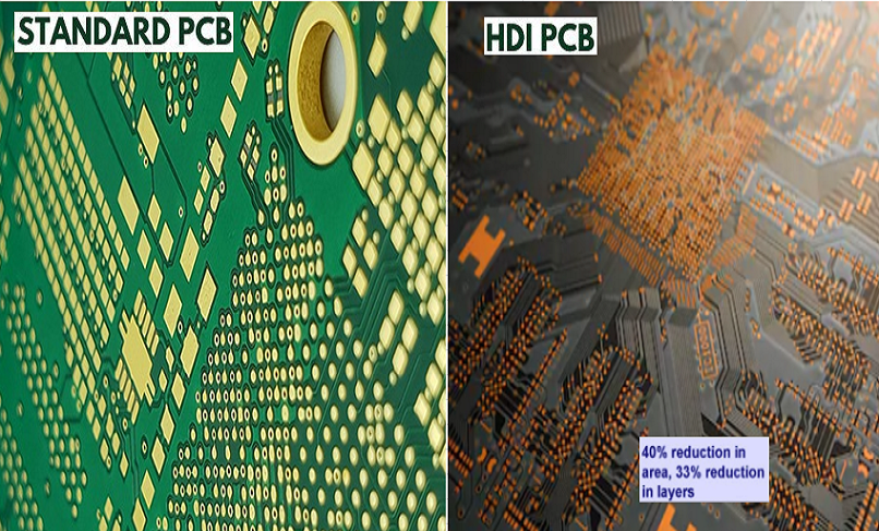
HDI PCB and standard PCB serve different engineering needs. A standard PCB is usually the right choice for general electronics, moderate component density, wider routing, lower cost, and simpler production. An HDI PCB, or high density interconnect PCB, is selected when the design needs fine-pitch BGA escape, laser microvias, blind or buried vias, smaller line spacing, higher component density, shorter signal paths, and improved routing efficiency in a limited board outline. The best choice depends on via technology, trace width, layer count, component pitch, signal speed, thermal demand, cost target, and the hdi pcb manufacturer capability. In practice, the wrong choice is not only a cost issue. A standard PCB forced into an HDI layout can fail routing, while an unnecessary HDI PCB can add lamination, drilling, plating, inspection, and lead-time risk without improving the final product.
HDI PCB
What an HDI PCB Means
An HDI PCB is a printed circuit board with higher routing density than conventional multilayer boards. It normally uses laser-drilled microvias, fine trace and space, blind vias, buried vias, via-in-pad, sequential lamination, and thin build-up dielectric layers. IPC-2226 is commonly associated with HDI structure guidance, while IPC-2221 provides generic printed board design requirements and IPC-6012 defines qualification and performance requirements for rigid printed boards, including multilayer boards with or without blind and buried vias.
Typical HDI PCB planning values include 75/75 micron trace and space for standard HDI routing, local 50/50 micron routing for fine-pitch BGA breakout, 75-125 micron laser microvias, 50-80 micron build-up dielectric, and controlled impedance targets such as 50 ohm single-ended, 85 ohm PCIe differential, 90 ohm USB differential, or 100 ohm Ethernet and LVDS differential.
Where HDI Adds Value
- Fine-pitch BGA escape where dogbone fanout cannot fit.
- Compact products where board outline cannot increase.
- High-speed interfaces where shorter transitions reduce via stubs.
- Dense processor, memory, RF, camera, AI, medical, and wearable modules.
- Designs where a standard through-via structure blocks too many routing channels.
- Products that need smaller size, lower weight, and fewer interconnects.
Standard PCB
What a Standard PCB Means
A standard PCB usually uses mechanically drilled through vias, wider trace and space, conventional FR-4 or high-Tg FR-4 laminate, fewer lamination cycles, and simpler inspection requirements. It can be single-sided, double-sided, or multilayer. For many industrial controls, consumer products, power supplies, basic IoT devices, and low-to-medium-speed electronics, standard PCB construction is still the most cost-effective and reliable choice.
A typical standard multilayer PCB may use 100/100 micron to 150/150 micron trace and space, 0.20-0.30 mm finished hole size, 0.45-0.60 mm via pad diameter, 1 oz copper, 4 to 8 layers, and a through-via structure. These values are easier to fabricate, inspect, repair, and scale compared with dense HDI circuit boards.
Where Standard PCB Works Better
- Products with enough board area for through-via routing.
- Component pitch at 0.8 mm BGA or larger, or mostly QFP, SOIC, SOT, and connectors.
- Cost-sensitive products where advanced microvias are not required.
- Low-to-medium speed circuits without strict transition loss requirements.
- High-current boards where wide copper and simple fabrication are more important than miniaturization.
- Prototype builds where speed and cost matter more than density.
Core Differences
Manufacturing Principle
The core difference between HDI PCB and standard PCB is how vertical interconnection is created. A standard PCB relies mainly on through vias that pass from top to bottom. These vias are easy to drill and plate, but they consume routing area on every layer. HDI PCB uses selected-layer vias, such as blind microvias and buried vias, so routing layers are blocked only where needed.
| Factor | HDI PCB | Standard PCB |
|---|---|---|
| Main interconnect | Laser microvias, blind vias, buried vias, via-in-pad | Mechanical through vias |
| Routing density | High | Moderate |
| Best package support | 0.4 mm to 0.5 mm BGA by review | 0.8 mm BGA and larger is easier |
| Fabrication complexity | Higher | Lower |
| Cost level | Higher per board | Lower per board |
| Best value | Miniaturization and high-speed density | Cost-effective general electronics |
Engineering Decision
The engineering decision should be based on routing feasibility and product-level value. If a standard PCB can route the design with stable impedance, enough test access, acceptable thermal performance, and the required board size, it is usually the better economic option. If the design cannot escape the BGA, cannot meet size limits, or suffers from long via stubs and blocked routing channels, HDI PCB becomes the stronger choice.
Via Technology
Via Size and Via Type
Via technology is the largest technical difference. Standard PCB fabrication uses mechanical drilling. HDI PCB fabrication uses laser drilling for microvias and may also use sequential lamination for multiple build-up layers. A through via may be easy to fabricate, but it blocks all layers and can create a long unused via stub. A blind microvia is shorter and occupies less space, but it requires tighter drilling, landing pad, plating, and inspection control.
| Via Feature | HDI PCB | Standard PCB |
|---|---|---|
| Common via type | Blind microvia, buried via, stacked or staggered microvia | Through via |
| Drilling method | Laser drilling plus mechanical drilling | Mechanical drilling |
| Typical laser microvia diameter | 75-125 microns | Not usually used |
| Typical mechanical finished hole | 0.15-0.25 mm by review | 0.20-0.35 mm common |
| Via aspect ratio | Microvia at or below 1:1 preferred | Mechanical via commonly 8:1 to 10:1 by capability |
| Routing effect | Selected layer connection saves space | Full-board connection blocks routing layers |
Blind and Buried Vias
Blind vias connect an outer layer to an internal layer. Buried vias connect internal layers only. These structures help HDI boards route dense packages without increasing layer count too much. They also reduce via stub length for high-speed signals. The tradeoff is extra lamination, tighter registration, more inspection, and higher cost.
Via-in-Pad
Via-in-pad is common in HDI designs using fine-pitch BGA, QFN thermal pads, or RF grounding. The via must be filled, capped, and planarized for reliable assembly. Open vias inside solder pads can wick solder during reflow and cause voids or weak joints. Standard PCB designs usually avoid via-in-pad unless space or thermal performance requires it.
Trace Width
Lines and Spaces
HDI PCB uses finer lines and spaces than standard PCB. This is necessary for dense BGA escape and compact routing. However, finer routing is not free. It requires tighter imaging, better etch control, thinner copper in fine-line areas, and stronger process monitoring.
| Routing Class | Trace / Space | Copper Thickness | Typical Use |
|---|---|---|---|
| Standard PCB | 100/100 to 150/150 microns | 18-35 microns | General electronics and industrial controls |
| Standard HDI PCB | 75/75 microns | 12-18 microns | Dense digital routing |
| Fine HDI breakout | 50/50 microns | 9-12 microns | 0.4 mm to 0.5 mm BGA escape |
| Advanced local HDI | Below 50/50 microns by qualification | 5-9 microns | Special high-density zones |
Copper and Etching Control
Trace width cannot be reviewed separately from copper thickness. A 50/50 micron region on 35 micron copper is much harder to etch than the same geometry on 9-12 micron copper. For cost-effective hdi pcb fabrication, fine traces should be limited to the BGA escape or high-density area instead of being used across the whole board.
Layer Count
Layer Strategy
A standard PCB may increase layer count to solve routing. An HDI PCB may reduce layer count by using microvias and selected-layer connections. However, the relationship is not automatic. A poorly planned HDI stackup can cost more than a conventional board with two additional layers.
| Stackup Option | Typical Structure | Best Use | Manufacturing Impact |
|---|---|---|---|
| Standard multilayer | 4 to 12 layers with through vias | General electronics | Lower cost and simpler lamination |
| 1+N+1 HDI | One build-up layer per side | Moderate density BGA | One sequential build-up level |
| 2+N+2 HDI | Two build-up layers per side | Dense BGA and high-speed modules | Higher cost and more registration control |
| 3+N+3 HDI | Three build-up layers per side | Very dense modules | High fabrication risk and cost |
| ELIC / any-layer HDI | Microvias across many layers | Extreme miniaturization | Highest density and strongest process demand |
Sequential Lamination
Sequential lamination is a major cost and yield factor in HDI PCB fabrication. Each build-up cycle adds drilling, plating, imaging, lamination, registration control, inspection, and schedule time. A standard PCB usually has fewer lamination cycles, so it is easier to control at volume.
Component Density
Package Pitch
Component density often decides whether HDI PCB is required. Standard PCB can handle many SMT components, connectors, and larger BGA packages. HDI becomes necessary when the board must route fine-pitch processors, memory, RF modules, compact sensors, and dense power management ICs within a small area.
| Component Condition | Standard PCB Fit | HDI PCB Fit |
|---|---|---|
| 0.8 mm BGA | Usually suitable | Suitable but may be unnecessary |
| 0.65 mm BGA | Possible with careful routing | Often easier and smaller |
| 0.5 mm BGA | Difficult with through vias | Common HDI use case |
| 0.4 mm BGA | Usually not practical for standard routing | Requires HDI review |
| QFN thermal pad | Possible with thermal vias | VIPPO may improve heat path |
| Dense camera or RF module | May need larger outline | Better routing density |
Board Size and Weight
HDI PCB can reduce product size by allowing components to sit closer together and by reducing routing escape area. This is valuable in handheld devices, wearables, medical sensors, compact industrial modules, AI camera boards, and communication products. A standard PCB is more suitable when enclosure space is not tight and cost is more important than miniaturization.
Signal Integrity
Shorter Transitions
HDI PCB can improve signal integrity by shortening layer transitions and reducing via stubs. This is useful for high-speed interfaces such as PCIe, USB, MIPI, LVDS, Ethernet, DDR, RF control lines, and camera links. Blind microvias create shorter electrical paths than long through vias, but they still require proper return-path planning and reference plane continuity.
| Signal Item | HDI PCB Advantage | Standard PCB Limitation |
|---|---|---|
| Via stub | Shorter with blind microvias | Longer through-via stubs |
| BGA escape | Shorter breakout path | Longer dogbone and layer transitions |
| Reference plane | Can be optimized with dense stackup | May be interrupted by through vias |
| Impedance control | Works well with planned stackup and coupons | Works well if routing space is enough |
| Crosstalk | Can be reduced after breakout | May increase if channels are crowded |
Controlled Impedance
Both HDI PCB and standard PCB can support controlled impedance. The difference is process sensitivity. HDI designs often use thinner dielectrics and finer traces, so pressed dielectric thickness, copper plating, solder mask, and imaging variation have stronger influence. The fabrication drawing should define target impedance, tolerance, routing layer, reference plane, material, copper thickness, and TDR coupon requirements.
Cost
Cost Structure
Standard PCB is usually cheaper because it uses wider lines, mechanical drilling, fewer lamination cycles, simpler materials, and easier inspection. HDI PCB costs more because of laser drilling, sequential lamination, finer imaging, via filling, tighter registration, more coupons, X-ray, and microsection inspection.
| Cost Driver | HDI PCB | Standard PCB |
|---|---|---|
| Drilling | Laser microvias plus mechanical drilling | Mechanical drilling |
| Lamination | Sequential build-up may be required | Fewer lamination cycles |
| Imaging | LDI often preferred for fine lines | Contact or standard LDI imaging |
| Inspection | X-ray, microsection, impedance coupons, E-test | AOI, E-test, standard inspection |
| Material | Thin dielectric and low-loss options may be needed | Standard FR-4 or high-Tg FR-4 |
| Lead time | Longer for complex builds | Shorter for standard builds |
When HDI Saves Money
HDI is more expensive at the bare-board level, but it can save money at the product level when it reduces board area, removes connectors, eliminates daughterboards, lowers layer count, shortens assembly time, or improves functional yield. The correct comparison is not only PCB price. It is total product cost, including assembly, enclosure size, failure rate, rework, and field reliability.
Feature Comparison
HDI PCB vs Standard PCB Table
| Feature | HDI PCB | Standard PCB |
|---|---|---|
| Via size | 75-125 micron laser microvias common | 0.20-0.35 mm mechanical vias common |
| Via type | Blind, buried, stacked, staggered, via-in-pad | Mostly through vias |
| Lines and spaces | 75/75 microns standard, 50/50 microns local | 100/100 to 150/150 microns common |
| Drilling method | Laser and mechanical drilling | Mechanical drilling |
| Layer count strategy | Uses build-up layers and microvias | Uses conventional multilayer routing |
| Component density | High | Moderate |
| Signal integrity | Shorter transitions and fewer stubs | Good when routing space is enough |
| Cost | Higher bare-board cost | Lower bare-board cost |
| Ideal for | Fine-pitch BGA, compact products, high-speed dense routing | General electronics, power boards, cost-sensitive products |
Simple Selection Logic
- Choose standard PCB when the design routes cleanly with through vias and wider traces.
- Choose HDI PCB when BGA escape, board size, signal integrity, or component density cannot be solved with standard routing.
- Use HDI features locally where possible instead of applying fine-line rules to the full board.
- Confirm the hdi pcb manufacturer capability before final layout.
- Compare total product cost, not only PCB fabrication cost.
When to Choose Which
Choose HDI PCB When
- The design uses 0.5 mm or 0.4 mm BGA packages.
- The enclosure limits PCB outline and connector placement.
- Through vias block too many routing channels.
- High-speed signals need shorter via transitions.
- The layout needs via-in-pad, blind vias, or buried vias.
- A smaller layer count can be achieved with HDI routing.
- The product value justifies higher fabrication cost.
Choose Standard PCB When
- The board has enough routing area.
- The design uses 0.8 mm BGA or larger packages.
- Cost and lead time are more important than miniaturization.
- The circuit is low-to-medium speed.
- The product does not need laser microvias.
- High current or simple power routing dominates the design.
- A standard multilayer stackup can meet all requirements.
Quality Control
HDI PCB Quality Checks
HDI PCB quality control must verify hidden structures and fine features. A bare board may pass electrical test but still fail at assembly if via-in-pad filling, copper plating, microvia reliability, solder mask registration, or impedance coupons are not controlled.
- Laser microvia diameter and depth inspection.
- Microvia aspect ratio review.
- X-ray for stacked and filled vias.
- Microsection for plating and dielectric verification.
- AOI for fine lines and spaces.
- TDR coupon testing for controlled impedance.
- Electrical test for opens and shorts.
- Warpage check for thin BGA-heavy designs.
- Surface finish thickness measurement.
- BGA assembly X-ray when via-in-pad is used.
Standard PCB Quality Checks
Standard PCB quality control is still important, but the risk profile is simpler. The main checks are mechanical drilling quality, plated through-hole integrity, conductor width, solder mask registration, surface finish, electrical test, and visual acceptability. IPC-6012 should be specified on the fabrication drawing along with class, copper requirements, surface finish, board thickness, and acceptance criteria.
Real Factory Case
Project Background
A customer developed a compact industrial AI camera controller using a 0.5 mm BGA processor, LPDDR memory, MIPI camera input, USB 3.0, Ethernet, PMIC, flash, and two board-to-board connectors. The first design attempt used a standard 8-layer through-via PCB to control cost.
| Item | Standard PCB Attempt | HDI PCB Revision |
|---|---|---|
| Board type | Standard multilayer PCB | HDI PCB |
| Layer count | 8 layers | 10 layers |
| Stackup | Through-via only | 2+6+2 HDI |
| BGA pitch | 0.5 mm | 0.5 mm |
| Trace / space | 100/100 microns | 50/50 local, 75/75 general |
| Via structure | Through vias | Blind microvias and buried core vias |
| Controlled impedance | USB only | USB, MIPI, Ethernet |
| Inspection | AOI and E-test | AOI, E-test, X-ray, microsection, TDR |
Problem Found
The standard PCB version could not escape the inner BGA rows without adding board area or increasing layer count. Several through vias blocked DDR and MIPI routing channels. Decoupling capacitors were placed 6-9 mm away from key power balls, and one USB differential pair crossed a reference-plane gap. The board could be forced to route, but it did not meet size, impedance, and assembly reliability targets.
- BGA fanout required too much routing area.
- Through-via fields blocked inner routing layers.
- USB impedance deviation reached +8.0% in review.
- DDR routes had poor reference-plane continuity.
- Board outline exceeded the enclosure limit by 7 mm.
- The first manufacturability review rejected two dense routing areas.
Improvement Result
The revised design used a 10-layer 2+6+2 HDI PCB. Laser microvias were used for the BGA escape, buried vias were used inside the core, and fine 50/50 micron routing was limited to the BGA region. General routing stayed at 75/75 microns to control cost and yield.
| Metric | Standard PCB Attempt | HDI PCB Revision |
|---|---|---|
| Board outline | 92 mm x 54 mm | 84 mm x 48 mm |
| BGA escape completion | Not acceptable | Completed |
| USB impedance deviation | +8.0% review estimate | +2.8% measured coupon |
| MIPI thermal soak failures | Not built for pilot | 0/160 |
| First-pass functional yield | Not released | 98.1% pilot yield |
| Estimated bare-board cost | Baseline 100% | 168% of baseline |
| Estimated system cost | Higher due to larger enclosure | Lower due to compact assembly |
The HDI PCB cost more as a bare board, but it allowed a smaller enclosure, cleaner BGA routing, better controlled impedance, and stable pilot assembly yield. The project showed why HDI should be selected by product-level engineering value, not only by board quotation.
Common Design Errors
HDI Selection Errors
- Choosing HDI because it sounds advanced, not because routing requires it.
- Using any-layer HDI when 1+N+1 or 2+N+2 would solve the design.
- Applying 50/50 micron routing across the whole board instead of only dense zones.
- Using stacked microvias where staggered vias would fit.
- Ignoring microvia aspect ratio before stackup approval.
- Forgetting X-ray and microsection requirements for filled via structures.
Standard PCB Selection Errors
- Forcing a 0.5 mm BGA into through-via routing without enough area.
- Increasing layer count repeatedly instead of reviewing HDI breakout.
- Ignoring via stubs on high-speed signals.
- Placing decoupling capacitors too far from fine-pitch BGA power pins.
- Assuming lower PCB cost means lower product cost.
- Skipping fabricator review before finalizing dense routing.
Documentation Errors
- No stackup drawing.
- No via structure map.
- No laser drill file for HDI.
- No IPC class on fabrication drawing.
- No impedance coupon definition.
- No via fill and cap notes for via-in-pad.
- No assembly drawing for fine-pitch BGA review.
FAQ
Question: What is the main difference between HDI PCB and standard PCB?
Answer: The main difference is interconnect density. HDI PCB uses microvias, blind vias, buried vias, via-in-pad, fine trace and space, and sequential lamination. Standard PCB mainly uses mechanically drilled through vias and wider routing rules.
Question: Is HDI PCB always better than standard PCB?
Answer: No. HDI PCB is better when the product needs fine-pitch BGA escape, smaller size, higher routing density, or shorter signal transitions. Standard PCB is better when the design has enough space, moderate density, lower speed, and strong cost pressure.
Question: Why does HDI PCB cost more?
Answer: HDI PCB costs more because it requires laser drilling, sequential lamination, finer imaging, tighter registration, via filling, X-ray, microsection, impedance coupons, and more detailed engineering review during fabrication.
Question: When should engineers switch from standard PCB to HDI PCB?
Answer: Engineers should switch to HDI PCB when a standard through-via design cannot route dense components, cannot meet board size, creates long high-speed stubs, blocks reference planes, or forces an inefficient layer count.


