
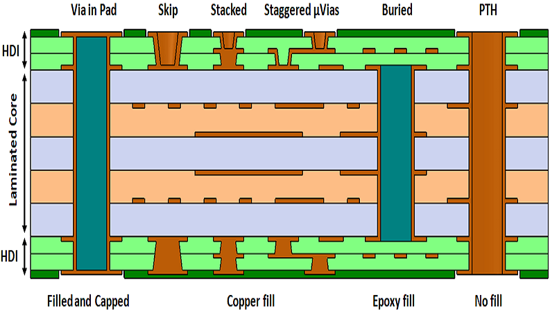
Blind via, buried via, and microvia are three different interconnect structures used to connect PCB layers without relying only on conventional through holes. A blind via connects an outer layer to an internal layer, a buried via connects only internal layers, and a microvia is a small laser-drilled via commonly used in high density interconnect boards. The correct choice depends on layer span, BGA pitch, trace density, signal speed, lamination sequence, cost target, and the hdi pcb manufacturer’s process window. In factory review, these vias are not interchangeable. Each type changes drilling method, copper plating risk, registration tolerance, inspection method, and final assembly reliability.
Blind Via
Definition and Layer Connection
A blind via starts from an outer PCB layer and ends at one or more internal layers. It does not pass through the full board thickness. It is called “blind” because one side is visible from the outside of the board and the other side terminates inside the stackup.
Typical blind via examples:
- L1 to L2 laser microvia
- L1 to L3 controlled-depth blind via
- L10 to L9 laser microvia
- Outer layer to inner signal layer
- Outer BGA pad to first routing layer
Blind vias are common in hdi pcb fabrication because they free internal routing channels that would otherwise be blocked by through vias.
Technical Parameters
| Blind Via Item | Practical Range | Engineering Meaning |
|---|---|---|
| Laser blind via diameter | 75-125 microns | Common HDI breakout range |
| Advanced laser via diameter | 50-75 microns by review | Dense BGA and compact modules |
| Mechanical blind via | 0.15-0.30 mm by review | Controlled-depth drilling |
| Microvia aspect ratio | 1:1 maximum preferred | Plating reliability limit |
| Preferred microvia ratio | 0.75:1 or lower | Better production margin |
| Common use | 0.4 mm to 0.5 mm BGA | Fine-pitch escape routing |
Buried Via
Definition and Layer Connection
A buried via connects internal PCB layers only. It does not reach the top or bottom surface. After lamination, it is hidden inside the board and cannot be seen from outside.
Typical buried via examples:
- L2 to L3
- L3 to L6
- L4 to L5
- Internal core via before final lamination
- Power or signal connection between internal layers
Buried vias are often built in an inner core first. The core is drilled, plated, inspected, and then laminated into the final multilayer board.
Technical Parameters
| Buried Via Item | Practical Range | Engineering Meaning |
|---|---|---|
| Mechanical buried via diameter | 0.15-0.30 mm common | Core drilling and plating |
| Core layer span | Usually internal layer pairs | Depends on stackup |
| Aspect ratio | Based on core thickness | Plating reliability control |
| Inspection | AOI, E-test, microsection | Hidden structure verification |
| Lamination impact | Adds process step | Higher cost and longer lead time |
| Common use | Internal routing density | Keeps outer layers free |
Microvia
Definition and HDI Role
A microvia is a small via, typically laser-drilled, used in HDI PCB structures. Microvias usually connect adjacent layers, such as L1 to L2 or L2 to L3. They may be blind, buried, stacked, staggered, or placed inside component pads.
Common microvia structures:
- Single-level blind microvia
- Staggered microvia
- Stacked copper-filled microvia
- Via-in-pad microvia
- Any-layer HDI microvia
A microvia is not defined only by being “small.” In production, it must also match dielectric thickness, laser drilling quality, plating capability, target pad size, and reliability class.
Technical Parameters
| Microvia Item | Practical Range | DFM Meaning |
|---|---|---|
| Diameter | 50-125 microns | Depends on laser and material |
| Depth | 40-100 microns | Based on dielectric thickness |
| Aspect ratio | At or below 1:1 preferred | Plating reliability |
| Target pad | 200-300 microns common | Registration margin |
| Fill option | Copper or resin by structure | Reliability and assembly control |
| Inspection | X-ray, microsection, E-test | Hidden defect control |
Key Comparison
Layers Connected and Visibility
| Feature | Blind Via | Buried Via | Microvia |
|---|---|---|---|
| Layers connected | Outer layer to inner layer | Inner layer to inner layer | Usually adjacent HDI layers |
| Visibility | Visible from one outer side | Not visible from outside | Depends on structure |
| Typical span | L1-L2, L1-L3, bottom-side equivalents | L2-L3, L3-L6, internal cores | L1-L2, L2-L3, stacked or staggered |
| Main purpose | BGA breakout and surface access | Internal routing management | High-density miniaturization |
| Common board type | HDI PCB and dense multilayer | Multilayer and HDI PCB | HDI PCB |
| Main risk | Depth and landing registration | Core plating and lamination | Plating, fill, and reliability |
Drilling Method and Cost
| Feature | Blind Via | Buried Via | Microvia |
|---|---|---|---|
| Drilling method | Laser or controlled-depth mechanical drilling | Mechanical drilling before lamination | Laser drilling |
| Cost level | Medium to high | Medium to high | Medium to high by count and stack |
| Process step | Outer build-up or controlled-depth process | Internal core process | Sequential build-up process |
| Inspection need | Microsection, E-test, X-ray where needed | AOI, E-test, microsection | X-ray, microsection, E-test |
| Best cost use | Use only where through vias block routing | Use only where internal routing needs it | Use for dense packages and short transitions |
Applications
Blind Vias
Blind vias are used when surface components need direct access to inner layers without using full through holes.
Typical applications:
- Fine-pitch BGA fanout
- Processor and memory escape routing
- Decoupling capacitor connections
- RF ground transitions
- High-speed layer changes
- Compact wearable and IoT modules
- Camera, sensor, and AI modules
Blind vias are a good choice when the design needs surface-level density but does not require complex internal-only connections.
Buried Vias
Buried vias are used when internal layers need connection without disturbing outer-layer routing.
Typical applications:
- Internal signal layer transitions
- Power distribution between inner planes
- Dense multilayer routing
- Layer management in 2+N+2 structures
- High-speed internal routing
- Compact industrial or communication boards
- Designs with limited component-side routing space
Buried vias should be used carefully because they add lamination and inspection cost. If a through via or blind via solves the problem, a buried via may not be necessary.
Microvias
Microvias are used where high density interconnect routing is required.
Typical applications:
- 0.4 mm and 0.5 mm BGA escape
- Mobile and wearable electronics
- Medical miniaturized devices
- High-speed computing modules
- RF and communication modules
- Stacked package routing
- HDI circuit boards with fine line/space
Microvias are often used together with via-in-pad when the component pitch is too tight for dogbone fanout.
Manufacturing Differences
Blind Vias
Common process flow:
- Prepare the outer build-up dielectric or target layer.
- Drill the blind via by laser or controlled-depth mechanical method.
- Clean and desmear the via.
- Plate copper into the via.
- Inspect via depth, landing, and plating.
- Continue imaging, etching, solder mask, and finish.
Factory controls:
- Laser energy control
- Target pad size
- Dielectric thickness
- Plating thickness
- Via depth
- Annular ring
- Registration after lamination
Buried Vias
Common process flow:
- Image and etch internal core layers.
- Drill buried vias in the core.
- Plate the buried vias.
- Inspect internal layers by AOI.
- Laminate the core into the final stackup.
- Continue with outer layers and final drilling.
- Run electrical test and microsection.
Factory controls:
- Core thickness
- Drill accuracy
- Plating continuity
- Inner-layer registration
- Lamination movement
- Microsection validation
- Electrical continuity
Microvias
Common process flow:
- Laminate build-up dielectric.
- Laser drill microvias.
- Remove debris and residue.
- Plate copper into the microvias.
- Fill if stacked or via-in-pad.
- Cap and planarize if required.
- Inspect by X-ray or microsection.
- Repeat if multiple build-up layers are used.
Factory controls:
- Laser via diameter
- Via taper
- Dielectric thickness
- Aspect ratio
- Copper filling quality
- Target pad registration
- Stacked via alignment
- X-ray and microsection results
Core Technical Design Rules
Via Size and Aspect Ratio
| Via Type | Typical Diameter | Aspect Ratio Rule | Manufacturing Note |
|---|---|---|---|
| Blind laser microvia | 75-125 microns | 1:1 maximum preferred | 0.75:1 gives better margin |
| Advanced microvia | 50-75 microns | Process-specific | Requires review |
| Mechanical buried via | 0.15-0.30 mm | Based on core thickness | Needs plating validation |
| Through via | 0.20-0.35 mm common | 8:1 to 10:1 common by capability | Simpler but blocks layers |
Microvia aspect ratio is one of the most important reliability points. A deep, narrow microvia may pass initial electrical test but fail after thermal cycling if plating is weak.
Trace Width, Clearance, and Pad Design
| Design Item | Common HDI Range | Purpose |
|---|---|---|
| Standard HDI trace/space | 75/75 microns | Dense routing |
| Fine BGA breakout | 50/50 microns | 0.4 mm to 0.5 mm BGA |
| Microvia capture pad | 200-300 microns | Registration margin |
| Mechanical via pad | 350-500 microns | Drill and annular ring margin |
| Drill-to-copper clearance | 150-250 microns by review | Prevents shorts |
| Impedance tolerance | ±10% common, ±5% tighter | High-speed control |
The hdi pcb manufacturer should approve these rules before routing. Changing pad size or dielectric thickness after layout can break both DFM and impedance control.
Cost and Lead Time
Cost Drivers
| Cost Driver | Blind Via | Buried Via | Microvia |
|---|---|---|---|
| Extra drilling | Medium | Medium | Medium to high |
| Sequential lamination | Possible | Often required | Often required |
| Fill and cap | Optional | Rare | Required for stacked or VIP |
| X-ray need | By structure | By risk | Common for stacked or filled |
| Lead time impact | Medium | Medium to high | Medium to high |
| Best cost control | Limit to dense zones | Use only where internal routing needs it | Avoid unnecessary stacking |
The cheapest via type is the one that solves the routing problem with the fewest extra process steps. A layout with too many unnecessary stacked microvias can cost more than a slightly larger standard via design.
Typical Lead Time Impact
| Board Structure | Typical Prototype Lead Time Impact |
|---|---|
| Standard through-via multilayer | Baseline |
| Blind via only | Add 2-4 working days |
| Buried via core | Add 3-6 working days |
| 1+N+1 microvia HDI | Add 4-7 working days |
| 2+N+2 HDI | Add 7-12 working days |
| Stacked filled microvia HDI | Add 10-15 working days |
Lead time depends on layer count, material stock, copper thickness, lamination cycles, inspection depth, and whether the design needs expedited fabrication.
Quality Control
Bare Board Inspection
Quality control must match the via structure. Hidden vias cannot be judged only by surface appearance.
Required checks:
- CAM and DFM review
- Stackup verification
- Drill file verification
- Laser drill inspection
- Inner-layer AOI
- Copper plating thickness measurement
- X-ray for stacked or filled microvias
- Microsection near critical via fields
- 100% electrical test
- TDR test for controlled impedance designs
- Thermal cycling for high-reliability applications
- Final visual inspection
IPC-2226 is the key HDI design reference for microvia and high density interconnect structures. IPC-6012 is used for rigid printed board performance and qualification requirements, including multilayer boards with or without blind and buried vias.
When to Choose Which
Choose Blind Via When
Use blind vias when:
- Outer-layer components need access to inner layers.
- BGA escape is difficult with through vias.
- The design needs shorter signal transitions.
- Through vias block too many routing channels.
- Decoupling must be placed close to power pins.
- Board outline cannot grow.
- Cost allows HDI processing but not full any-layer HDI.
Blind vias are often the first HDI upgrade from a standard multilayer board.
Choose Buried Via When
Use buried vias when:
- Internal layers need connection without outer-layer access.
- Outer layers must stay free for components or fine traces.
- The stackup already requires internal core processing.
- Through vias create too much routing blockage.
- Internal signal routing needs cleaner layer management.
- The design can justify extra lamination cost.
Buried vias are powerful, but they are not always necessary. They should be used only where they solve a clear routing or layer-management problem.
Choose Microvia When
Use microvias when:
- BGA pitch is 0.5 mm or smaller.
- Routing density exceeds mechanical via capability.
- Via-in-pad is required.
- High-speed signals need short layer transitions.
- Product size must be minimized.
- The design uses 1+N+1, 2+N+2, or any-layer HDI.
- Sequential build-up is already part of the stackup.
Microvias are best for dense HDI zones. They should not be added across the entire board without a routing reason.
Two Key Comparisons
Blind Via vs Buried Via
| Item | Blind Via | Buried Via |
|---|---|---|
| Visible from outside | Yes, one side | No |
| Layer connection | Outer to inner | Inner to inner |
| Main use | BGA fanout and surface routing | Internal layer management |
| Fabrication timing | Outer build-up or controlled-depth process | Before final lamination |
| Cost impact | Medium to high | Medium to high |
| Best design reason | Saves surface and routing space | Keeps internal connections hidden |
Microvia vs Mechanical Via
| Item | Microvia | Mechanical Via |
|---|---|---|
| Drilling method | Laser drilling | Mechanical drilling |
| Diameter | 50-125 microns common | 0.20-0.35 mm common |
| Best use | HDI and fine-pitch BGA | General routing and power |
| Aspect ratio | 1:1 maximum preferred | 8:1 to 10:1 common by capability |
| Layer span | Usually adjacent layers | Can span full board |
| Cost | Higher per structure | Lower per structure |
| Main risk | Fill, plating, registration | Stub length and layer blockage |
Real Factory Case
Project Background
A compact industrial vision controller used a 0.5 mm BGA processor, LPDDR memory, PMIC, USB 3.0, MIPI camera input, Ethernet PHY, and two board-to-board connectors. The first layout used mostly through vias and limited blind vias.
| Item | First Design | Revised HDI Design |
|---|---|---|
| Board type | Standard multilayer attempt | HDI PCB |
| Layer count | 8 layers | 10 layers |
| Stackup | Through-via only | 2+6+2 |
| BGA pitch | 0.5 mm | 0.5 mm |
| Trace/space | 100/100 microns | 50/50 local, 75/75 general |
| Blind vias | Not used | L1-L2 and L10-L9 |
| Buried vias | Not used | L3-L6 core zones |
| Microvias | Not used | 90 micron laser microvias |
| Inspection | AOI and E-test | AOI, E-test, X-ray, microsection, TDR |
Problem Found
The first design could not complete BGA escape without increasing board outline by 12 mm. Several high-speed signals were forced through long through vias. DDR and MIPI routes crossed crowded routing channels, and decoupling capacitors moved too far from key power pins.
Pilot review found:
- 0.5 mm BGA escape was incomplete.
- Through vias blocked two internal routing channels.
- USB transition had excessive via stub length.
- PMIC decoupling loop length exceeded internal target.
- Board outline exceeded enclosure limit.
- Impedance coupon plan did not match real routing layers.
Corrective Result
The revised design used blind microvias for BGA breakout, buried vias for internal routing, and staggered microvias in less critical zones. Stacked microvias were kept only under the densest BGA escape region.
| Metric | First Design | Revised HDI Design |
|---|---|---|
| BGA escape completion | Not completed | Completed |
| Board outline | 96 mm x 58 mm | 84 mm x 50 mm |
| USB impedance deviation | Not released | +2.9% measured |
| Decoupling loop length | 7.5 mm max | 2.8 mm max |
| Marginal microvia findings | Not applicable | 0 panels |
| First-pass functional yield | Not released | 98.0% pilot |
| Estimated bare-board cost | Baseline 100% | 158% of baseline |
| Estimated system cost | Higher due to enclosure | Lower after outline reduction |
The HDI board cost more as a bare PCB, but the system cost improved because the enclosure became smaller, the routing was completed, and the high-speed interfaces passed validation.
Common Design Errors
Via Selection Errors
- Using buried vias where blind vias are enough.
- Using stacked microvias where staggered microvias would fit.
- Using through vias under fine-pitch BGA fields.
- Treating all microvias as automatically reliable.
- Forgetting via fill and cap requirements for via-in-pad.
- Mixing via structures without stackup planning.
Manufacturing Data Errors
- Missing laser drill files.
- No via structure map.
- No stackup drawing.
- No microvia aspect ratio review.
- No target pad size approval.
- No microsection coupon requirement.
- No X-ray requirement for stacked microvias.
- No impedance coupon for high-speed nets.
Assembly Errors
- Open via-in-pad used under BGA pads.
- Solder mask opening not matched to filled vias.
- No BGA X-ray after assembly.
- Decoupling capacitors placed too far from BGA power pins.
- Reflow warpage not measured.
- Bare-board E-test treated as final reliability proof.
FAQ
Question: What is the difference between blind via, buried via, and microvia?
Answer: A blind via connects an outer layer to an inner layer. A buried via connects only internal layers and is hidden inside the PCB. A microvia is a small laser-drilled via used in HDI PCB designs, usually between adjacent layers.
Question: Is a microvia always a blind via?
Answer: A microvia is often a blind via when it connects an outer layer to the next inner layer, such as L1 to L2. However, microvias can also be stacked, staggered, buried, or used in any-layer HDI structures depending on the stackup.
Question: Which via type is most expensive?
Answer: The most expensive option is usually not one via type alone but the full structure. Stacked, filled microvias with sequential lamination often cost more than simple blind or buried vias because they require copper fill, planarization, X-ray, and microsection inspection.
Question: When should engineers choose microvias instead of standard vias?
Answer: Engineers should choose microvias when fine-pitch BGA escape, compact board size, short signal transitions, via-in-pad, or high density interconnect routing cannot be achieved with standard mechanical through vias.


