







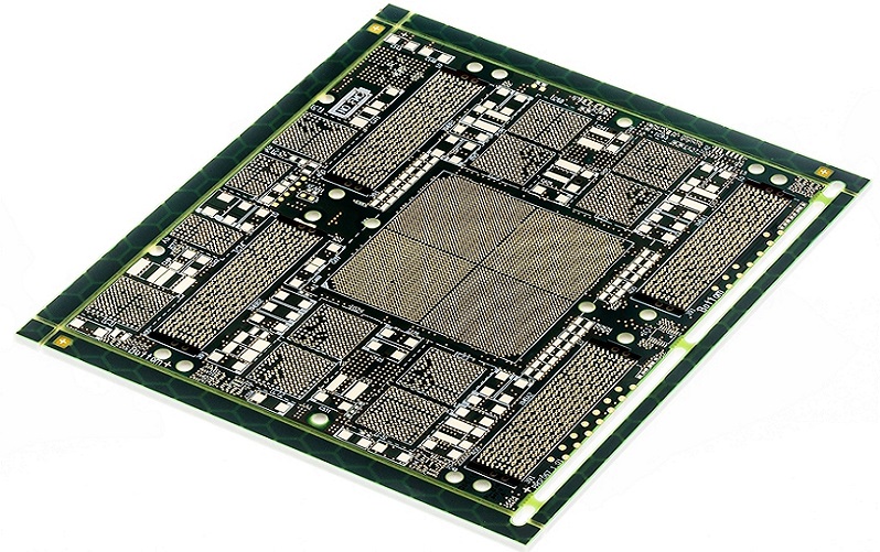
High density interconnect (HDI) PCB technology increases routing density by combining laser microvias, fine conductor geometries, sequential lamination, thin dielectric materials, and optimized stack-up planning. A successful HDI PCB design is not determined by layout density alone. The final manufacturing yield depends on whether trace width, microvia geometry, impedance targets, material selection, copper thickness, lamination sequence, and fabrication capability are defined together before routing begins. When the PCB designer and HDI PCB manufacturer collaborate during the early design stage, fabrication yield can typically improve by more than 10%, impedance variation can be reduced below ±7%, and unnecessary sequential lamination cycles can often be eliminated.
A production-ready HDI PCB package should clearly define:
- Layer stack-up
- Build-up sequence
- Microvia structure
- Via in pad requirements
- Controlled impedance
- Finished copper thickness
- Base material
- Surface finish
- Sequential lamination count
- Reliability requirements
- IPC acceptance class
- Electrical testing requirements
IPC-2221 provides the general requirements for printed circuit board design, IPC-2226 defines design practices for HDI printed boards, and IPC-6012 specifies qualification and performance requirements for rigid printed circuit boards containing microvias and blind/buried vias. Official standards are available through the IPC website.
HDI PCB Design Specifications
Trace and Space
Trace width and spacing determine routing density, manufacturing yield, and impedance stability.
Typical production capabilities are shown below.
| Manufacturing Level | Trace / Space |
|---|---|
| Standard PCB | 100/100 μm (4/4 mil) |
| Conventional HDI | 75/75 μm (3/3 mil) |
| Advanced HDI | 60/60 μm |
| Ultra HDI | Below 50/50 μm |
For most networking, AI computing and communication products:
- Finished copper: 18–35 μm
- Outer copper after plating: 30–38 μm
- Etching tolerance: ±10–15 μm
- AOI inspection resolution: 10 μm
Reducing copper thickness before imaging significantly improves fine-line yield because lateral etching becomes easier to control.
Microvia Diameter
Laser microvias occupy much less routing area than conventional through holes.
Typical manufacturing parameters include:
- Laser drill diameter:
- 60 μm
- 75 μm
- 100 μm
- 125 μm
- Finished diameter:
- 50–100 μm
- Capture pad:
- 180–300 μm
- Laser dielectric depth:
- 50–100 μm
Recommended aspect ratio:
0.75:1 to 1:1
Copper filled microvias normally require:
- Complete bottom coverage
- No internal void
- Surface dimple below 20 μm
Stack-Up Formats
Common HDI stack-up structures include:
| Stack-up | Total Layers | Typical Application |
|---|---|---|
| 1+4+1 | 6 | Consumer electronics |
| 1+6+1 | 8 | Communication boards |
| 2+4+2 | 8 | Fine-pitch BGA |
| 2+6+2 | 10 | AI modules |
| 3+8+3 | 14 | High-speed computing |
| Every Layer Interconnect | Variable | Smartphones and advanced processors |
The notation represents:
- i = Build-up layers
- N = Core layers
Example:
2+6+2
means
- Two build-up layers
- Six-layer core
- Total ten copper layers
The stack-up should always remain symmetrical around the center layer to minimize bow and twist during lamination.
Best Practices for Layout
Via in Pad
Via in Pad places laser microvias directly inside BGA pads.
Typical design values:
- 0.40 mm BGA pitch
- 75 μm laser via
- 200 μm capture pad
- Copper-filled microvia
- Planarized surface
Advantages include:
- Shorter signal path
- Better escape routing
- Lower inductance
- Smaller PCB size
However, Via in Pad requires:
- Copper filling
- Surface planarization
- Flat ENIG or ENEPIG finish
Poor filling may create solder voids during assembly.
Stack-Up Planning
Stack-up planning should begin before PCB routing.
The following parameters must be frozen before layout:
- Material type
- Dk
- Df
- Copper weight
- Build-up count
- Microvia structure
- Impedance target
- Reference planes
Changing dielectric thickness after routing usually requires complete impedance recalculation.
Typical HDI materials include:
- FR-4 High Tg 170°C
- Low-loss FR-4
- Megtron series
- Panasonic R-5775
- Isola I-Speed
Signal Integrity
HDI PCB design is closely related to signal integrity.
Typical controlled impedance:
| Signal Type | Target Impedance |
|---|---|
| Single-ended | 50Ω |
| Differential USB | 90Ω |
| PCI Express | 85Ω |
| Ethernet | 100Ω |
Typical impedance tolerance:
±7%
High-speed routing principles include:
- Continuous reference plane
- Minimum via transitions
- Differential length matching
- Short return path
- Back drilling where required
- Eliminate via stubs
For PCIe Gen5 or Gen6 routing, unnecessary via transitions can increase insertion loss more than the conductor itself.
Early Manufacturer Collaboration
One of the largest production mistakes is sending completed Gerber files to the factory before discussing manufacturing capability.
Early collaboration allows engineers to optimize:
- Stack-up
- Lamination cycles
- Material availability
- Laser capability
- AOI limits
- Registration tolerance
- Copper balancing
- Yield prediction
Factories often recommend increasing capture pad diameter by only 20–30 μm, improving production yield without affecting routing density.
HDI PCB Manufacturing Steps
Inner Layer Imaging & Etching
Manufacturing begins with the core.
Typical process:
- Copper cleaning
- Dry film lamination
- Direct imaging
- UV exposure
- Developing
- Acid etching
- AOI
Typical production values:
- Inner copper:
18 μm - Finished trace tolerance:
±10 μm - Registration:
±25 μm
AOI identifies opens, shorts, missing copper and over-etch before lamination.
Sequential Lamination
Sequential lamination builds HDI structures layer by layer.
Typical process:
Core
↓
Lamination
↓
Laser drilling
↓
Copper plating
↓
Imaging
↓
Second lamination
↓
Laser drilling
↓
Copper filling
↓
Outer layers
Each additional lamination introduces material movement.
Factories therefore compensate artwork separately for every build-up cycle rather than using identical scaling.
Typical lamination parameters:
- 185–205°C
- Vacuum pressure
- Controlled cooling
- Resin flow verification
Laser Microvia Drilling
Laser drilling produces blind microvias.
Typical controls:
- Hole diameter:
60–100 μm - Position tolerance:
±20 μm - Dielectric removal:
100% - No resin residue
Modern UV laser systems inspect each drilled hole immediately after processing.
Typical inspection includes:
- Diameter
- Roundness
- Bottom copper exposure
- Debris
Via Plating & Filling
After laser drilling:
- Desmear
- Electroless copper
- Electroplating
- Copper filling
- Planarization
Quality targets:
- Void-free filling
- Uniform thickness
- Bottom copper >20 μm
- Surface dimple <15 μm
Pulse plating provides better copper distribution than conventional DC plating for stacked microvias.
Repeating the Build-Up
Multiple build-up layers require repeating:
Laser drill
↓
Copper plating
↓
Copper filling
↓
Planarization
↓
Imaging
↓
Etching
↓
Inspection
A 3+N+3 board may require three independent laser drilling cycles and three lamination processes.
Artwork compensation is recalculated after every build-up stage because resin expansion differs slightly after each press cycle.
Outer Layer & Surface Finish
After all HDI layers are completed:
- Outer imaging
- Copper plating
- Pattern plating
- Final etching
- Solder mask
- Surface finish
- Legend
- Routing
- Electrical testing
Typical finishes:
| Surface Finish | Typical Application |
|---|---|
| ENIG | High-speed BGA designs |
| ENEPIG | Wire bonding and advanced packaging |
| OSP | Consumer electronics |
| Immersion Silver | RF and microwave circuits |
| Immersion Tin | Fine-pitch SMT assembly |
Surface flatness is especially important for Via in Pad structures.
Every Layer Interconnect
Every Layer Interconnect (ELIC) allows microvias between every adjacent copper layer.
Instead of only connecting build-up layers,
L1
↓
L2
↓
L3
↓
L4
↓
…
↓
Ln
can all be connected using laser microvias.
Advantages include:
- Maximum routing density
- Short signal path
- Lower inductance
- Smaller PCB size
- Better BGA escape
Manufacturing challenges include:
- Multiple laser cycles
- Registration accumulation
- Higher plating demand
- Increased inspection requirements
ELIC is widely used in smartphones, AI processors and advanced wearable electronics.
Quality Control
Critical inspections include:
| Inspection | Target |
|---|---|
| Laser Hole Diameter | ±10 μm |
| Registration | ±25 μm |
| Copper Thickness | Within drawing specification |
| Microvia Filling | No voids |
| Copper Dimple | <20 μm |
| Controlled Impedance | ±7% |
| Electrical Test | 100% Pass |
Reliability validation includes:
- Thermal cycling
- Cross-section analysis
- CAF testing
- IST testing
- Solder float
- Reflow simulation
- X-ray inspection
- Microsection analysis
A production lot should never rely solely on AOI. Cross-section measurements remain the only reliable method for verifying copper thickness at the microvia knee and via bottom.
Factory Case Study
16-Layer AI Accelerator Board
Structure:
- 16 Layers
- 3+10+3 Stack-up
- 0.40 mm BGA
- 75 μm microvia
- 75/75 μm trace & space
- 50Ω / 100Ω impedance
- ENIG finish
Initial Problems:
- Registration shift:
48 μm - Impedance deviation:
+11% - Microvia void rate:
6.4% - Yield:
89.1%
Root Causes:
- Artwork compensation identical for all lamination cycles
- Copper plating too thick
- Differential impedance modeled using base copper
- Laser energy inconsistent on edge panels
Corrective Actions:
- Independent compensation for every lamination
- Pulse reverse plating
- Finished copper impedance recalculation
- Edge panel laser calibration
- Additional microsection coupons
Results:
| Item | Before Improvement | After Improvement |
|---|---|---|
| Registration | 48 μm | 24 μm |
| Microvia Void Rate | 6.4% | 0.8% |
| Impedance Variation | +11% | ±5.8% |
| Production Yield | 89.1% | 98.5% |
| Scrap Rate | 10.9% | 1.6% |
The largest improvement came from separating artwork scaling for each build-up cycle rather than using a single compensation factor for the entire panel. This reduced cumulative registration error and improved copper capture on stacked microvias without changing the PCB layout.
Common Design Errors
Designing Without Manufacturing Capability
Many HDI PCB layouts are completed before confirming the manufacturer’s actual fabrication capability. This often forces expensive engineering changes after the PCB has already entered CAM review.
Typical mismatches include:
- Designing 50/50 μm trace and space when the factory capability is 60/60 μm
- Using 60 μm laser microvias while the supplier only qualifies 75 μm
- Selecting four stacked microvias although only two stacked levels are production qualified
- Specifying copper-filled Via in Pad without including planarization requirements
- Choosing asymmetric stack-ups that exceed the manufacturer’s lamination capability
Production engineers typically review the following items before approving HDI fabrication:
- Minimum conductor width
- Minimum spacing
- Laser drilling capability
- Registration tolerance
- Copper filling process
- Sequential lamination capability
- AOI resolution
- Electrical testing method
If these parameters are verified during stack-up planning instead of after routing, production yield generally improves significantly while reducing engineering review time.
Excessive Stacked Microvias
Stacked microvias provide the highest routing density but should not be used everywhere.
For example:
- Three-level stacked microvias beneath every BGA pad dramatically increase copper filling difficulty.
- Four-level stacked structures require additional sequential lamination and create greater thermal stress.
- Long vertical copper columns become more sensitive to plating voids and registration error.
Many experienced HDI PCB manufacturers limit stacked microvias to only the highest-density component areas and replace the remaining transitions with staggered microvias.
A practical optimization strategy is:
- Critical processor BGA → stacked microvias
- Memory devices → staggered microvias
- Peripheral interfaces → blind vias
- Low-speed routing → through holes
This approach reduces manufacturing cost without sacrificing routing density.
Poor Return Path Planning
Signal routing alone does not guarantee signal integrity.
Common design mistakes include:
- Routing differential pairs across split reference planes
- Removing ground copper beneath high-speed signals
- Excessive layer transitions
- Missing return vias beside signal vias
- Long parallel routing between noisy power circuits and sensitive data signals
Typical design targets:
- Continuous reference plane beneath every controlled impedance trace
- Return vias within 1.0 mm of every signal via
- Differential skew below 5 ps
- Pair length matching within 5 mil for PCIe Gen5 and similar interfaces
Ignoring the return current path often produces larger impedance discontinuities than the trace geometry itself.
Incorrect Copper Thickness Assumptions
Many impedance failures originate from modeling base copper instead of finished copper.
Example:
Design assumption:
- Base copper = 18 μm
Actual finished copper:
- Base copper = 18 μm
- Pattern plating = 18 μm
- Finished copper ≈ 36 μm
The increased conductor thickness lowers characteristic impedance.
Typical consequences include:
- 50 Ω design measuring 46–47 Ω
- Differential impedance below specification
- Increased insertion loss variation
- Additional PCB scrap
Field solvers should always calculate impedance using finished copper thickness supplied by the HDI PCB manufacturer.
Ignoring Resin Flow During Lamination
Sequential lamination changes dielectric thickness because resin flows under heat and pressure.
Typical resin flow ranges:
- 8–20%
Factors affecting flow include:
- Glass style
- Resin content
- Copper balance
- Panel density
- Press pressure
- Heating rate
Ignoring resin flow may result in:
- Impedance variation
- Layer thickness inconsistency
- Registration movement
- Local resin starvation
Experienced PCB fabrication engineers usually predict resin movement during stack-up design rather than correcting problems after pilot production.
Manufacturing Quality Control
Critical Process Inspection
HDI PCB manufacturing requires inspection after every major process instead of relying only on final electrical testing.
Typical process controls include:
| Manufacturing Stage | Inspection Method | Acceptance Target |
|---|---|---|
| Inner Layer Imaging | AOI | No opens or shorts |
| Laser Drilling | Vision Inspection | Hole position within ±20 μm |
| Desmear | Microsection | Complete resin removal |
| Copper Plating | Thickness Measurement | Uniform plating within specification |
| Via Filling | X-ray & Microsection | No voids or seam cracks |
| Sequential Lamination | Registration Measurement | Within ±25 μm |
| Fine Line Etching | AOI | Trace tolerance ±10–15 μm |
| Final Electrical Test | Flying Probe / Fixture Test | 100% Pass |
Reliability Verification
Production qualification commonly includes:
- Thermal cycling
- Solder float testing
- IST (Interconnect Stress Test)
- Cross-section analysis
- Peel strength
- CAF resistance
- Moisture resistance
- Electrical isolation testing
Typical qualification targets:
| Test Item | Typical Requirement |
|---|---|
| Thermal Cycling | 500–1000 cycles |
| Solder Float | 288°C × 10 seconds |
| Lead-Free Reflow Simulation | Three reflow cycles |
| CAF Resistance | No conductive filament growth |
| Electrical Continuity | 100% Pass |
Cross-section analysis should verify:
- Copper thickness at the microvia knee
- Copper thickness at the via bottom
- Dielectric thickness
- Resin recession
- Pad alignment
- Via filling quality
- Layer registration
HDI PCB Design Workflow
A production-oriented HDI PCB development process normally follows this sequence:
- Component placement
- HDI stack-up planning
- Material selection
- Controlled impedance calculation
- Fanout planning
- Via technology selection
- Differential routing
- Power distribution routing
- DFM review
- Manufacturer capability confirmation
- CAM optimization
- HDI PCB fabrication
- PCB assembly validation
- Reliability qualification
Skipping stack-up planning and moving directly to routing is one of the most common causes of redesign.
FAQ
What is the difference between a standard PCB and an HDI PCB?
Question: Why should engineers choose an HDI PCB instead of a conventional multilayer board?
Answer: An HDI PCB uses laser microvias, blind vias, buried vias, finer conductor geometries, and sequential lamination to increase routing density. Compared with conventional multilayer PCBs, HDI technology supports finer-pitch BGAs, shorter signal paths, lower parasitic inductance, and improved signal integrity while reducing overall board size.
When should Via in Pad be used?
Question: Is Via in Pad necessary for every HDI PCB?
Answer: No. Via in Pad is generally recommended for BGAs with pitches of 0.50 mm and below, especially 0.40 mm and 0.35 mm packages where conventional fanout is no longer practical. The microvia should normally be copper-filled and planarized before ENIG or ENEPIG surface finishing to prevent solder voids and ensure coplanarity.
How many sequential laminations are acceptable?
Question: Does increasing sequential lamination always improve routing density?
Answer: Additional sequential lamination increases routing flexibility but also raises fabrication complexity, material movement, registration error, manufacturing cost, and cycle time. Most networking, industrial, and automotive HDI products use one or two build-up cycles per side. Three or more build-up cycles are typically reserved for advanced computing, AI accelerators, aerospace, or substrate-like applications.
What is Every Layer Interconnect (ELIC)?
Question: How is Every Layer Interconnect different from a conventional HDI stack-up?
Answer: Every Layer Interconnect (ELIC) allows adjacent copper layers throughout the entire PCB to be interconnected with laser microvias instead of restricting microvias to the outer build-up layers. This architecture significantly improves routing density and shortens signal paths, making it suitable for smartphones, advanced AI processors, wearable electronics, and other ultra-compact designs. However, it requires multiple laser drilling cycles, repeated copper filling, precise sequential lamination, and extremely tight registration control, resulting in higher manufacturing complexity and cost.

![Understanding PCB Costs & Pricing [Your Complete Guide]](https://hdicircuitboard.com/wp-content/uploads/elementor/thumbs/Understanding-PCB-Costs-Pricing-Your-Complete-Guide-qzzhe6mcaxuolkux3xalfktgavumi9y1aqfbs9bpv4.webp "Understanding PCB Costs & Pricing [Your Complete Guide]")