







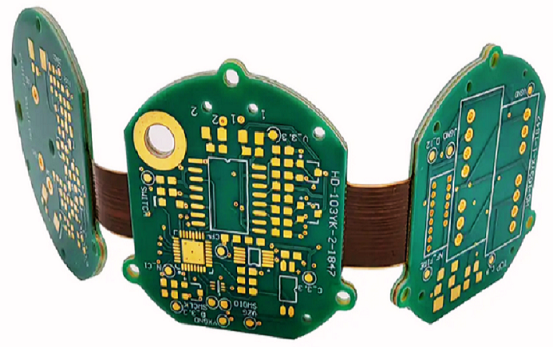
Reliable rigid-flex PCB design begins by treating the flexible section as a mechanical structure rather than as a thin rigid PCB. The design must define whether each bend is static or dynamic, calculate bend radius from finished flex pcb thickness, keep vias and components outside bending areas, select suitable polyimide and copper, balance the stack-up, stagger traces, reinforce pad transitions, and control the rigid-to-flex interface. When these rules are applied before rigid-flex PCB fabrication, engineers can reduce copper cracking, coverlay separation, impedance drift, assembly damage, and field failures.
A practical rigid-flex PCB design package should include:
- Separate rigid and flex stack-up regions
- Finished flex thickness
- Bend angle and bend direction
- Static or dynamic bend classification
- Minimum bend radius
- Installed three-dimensional shape
- Coverlay and stiffener drawings
- Copper type and thickness
- Impedance requirements
- Fabrication and reliability test criteria
IPC-2223 establishes sectional design requirements for flexible and rigid-flex printed boards, while IPC-6013 covers qualification and performance requirements for flexible and rigid-flex products designed to IPC-2221 and IPC-2223.
Bend Radius
Bend Radius Calculation
Bend radius is measured from the inside surface of the flex section to the center of the bend. A larger radius distributes mechanical strain across a wider area, while a smaller radius concentrates tensile and compressive stress in the copper and dielectric.
A practical starting point is:
| Flex Construction | Static Bend Radius | Dynamic Bend Radius |
|---|---|---|
| Single-layer flex | 6–10× flex thickness | 50–100× flex thickness |
| Double-layer flex | 10× flex thickness | 100–150× flex thickness |
| Multilayer flex | 12–20× flex thickness | Normally avoided |
| Rigid-flex transition | 10× flex thickness or greater | Application-dependent |
For a 0.15 mm double-layer flex section:
- Static starting radius: approximately 1.5 mm
- Conservative dynamic radius: approximately 15–22.5 mm
- Bend angle: normally kept at or below 90° for repetitive movement
Published rigid-flex design guidance commonly distinguishes approximately 10:1 static ratios from much larger 100:1 or 150:1 dynamic ratios because repeated cycling causes copper work hardening.
Finished Thickness Control
Bend calculations must use the completed flex construction, including:
- Polyimide core
- Copper
- Adhesive
- Coverlay
- Coverlay adhesive
- Plated copper where present
Example finished construction:
| Layer | Thickness |
|---|---|
| Coverlay polyimide | 25 µm |
| Coverlay adhesive | 25 µm |
| Rolled annealed copper | 18 µm |
| Polyimide core | 25 µm |
| Rolled annealed copper | 18 µm |
| Coverlay adhesive | 25 µm |
| Coverlay polyimide | 25 µm |
| Total nominal thickness | 161 µm |
A design calculated from only the 25 µm polyimide core would severely underestimate strain. Material tolerance and adhesive flow can also change the final thickness by approximately ±10–20 µm.
Bending Areas
Static Bends
A static bend is formed during assembly and then remains in one installed position. Typical examples include camera modules, compact medical instruments, and folded controller assemblies.
Static regions can normally support:
- One or two flex copper layers
- 6–10× thickness radius for simple structures
- 90° or 180° installation bends when the radius is controlled
- Limited assembly adjustments
The bend should be formed around a controlled tool rather than folded directly by hand. A 180° fold should not become a sharp crease. For a 0.20 mm two-layer flex section, a 2.0 mm or larger inside radius is a safer production starting point than a near-zero fold.
Dynamic Bends
Dynamic bends move repeatedly during operation. Typical examples include printer heads, robotic joints, sliding controls, and hinged electronics.
Dynamic regions should normally use:
- One copper layer where possible
- Two copper layers only after cycle-life validation
- Rolled annealed copper
- Adhesiveless polyimide
- Constant trace width
- Large bend radius
- No plated holes or components
- No heavy copper planes
Dynamic flex designs should also define:
- Required cycles: 10,000, 100,000, or more than 1,000,000
- Bend frequency
- Operating temperature
- Bend angle
- Flex length
- Torsion or twisting
- Installation tension
Static vs Dynamic Bends
| Design Factor | Static Bend | Dynamic Bend |
|---|---|---|
| Movement | Installation only | Repeated operation |
| Typical copper layers | 1–2 | Preferably 1 |
| Bend radius | 6–20× thickness | 50–150× thickness |
| Copper type | Rolled annealed or selected electrodeposited copper | Rolled annealed copper |
| Trace stacking | Limited | Strongly avoided |
| Validation | Assembly inspection | Cycle-life testing |
| Main failure risk | Creasing or delamination | Copper fatigue |
No Vias
Via Keep-Out Rules
Plated holes create rigid local structures that cannot stretch uniformly with the surrounding flex. A via in a bending area introduces:
- Copper barrel stress
- Pad lifting
- Annular-ring cracking
- Local stiffness
- Coverlay stress concentration
Practical design rules include:
- No plated through-holes inside the active bend
- No laser microvias inside a dynamic bend
- Keep via pads at least 1.0–2.0 mm from the bend tangent
- Keep drilled holes at least 1.27 mm from the rigid-to-flex boundary where space permits
- Increase clearance for high-cycle designs
Design guidance consistently excludes vias from active bending areas and recommends additional clearance around transition regions.
Pad Anchoring Outside Bends
When a via or component pad must sit close to the flex region:
- Use teardrops at trace-to-pad transitions
- Add copper anchoring where approved
- Extend coverlay over the trace shoulder
- Avoid locating the pad on the bend tangent
- Keep the pad on a mechanically supported area
A 0.20 mm finished via with a 0.45 mm pad may be manufacturable in a rigid area, but it should not be placed where the flex repeatedly bends.
No Sharp Angles
Curved Trace Geometry
Sharp trace corners concentrate mechanical stress. In rigid-flex PCB design, bend-region traces should use:
- Curved arcs
- Large-radius corners
- Two 45° bends where arcs are unavailable
- Smooth width transitions
- Constant copper cross-section
A practical trace corner radius is at least three times the trace width. For a 0.10 mm trace, a 0.30 mm radius reduces localized strain compared with a 90° corner.
Flex Outline Geometry
Sharp internal outline corners can start tears in polyimide and coverlay. Use:
- Internal corner radius of 0.75–1.50 mm
- Circular reliefs at flex cutout ends
- Rounded flex-tail edges
- Smooth neck transitions
- No narrow slots ending in square corners
For laser-cut flex profiles, even a 0.25 mm radius is better than a true corner, but larger radii provide better tear resistance.
Stack-Up Rules
Symmetry
A balanced rigid-flex stack-up reduces bow, twist, and lamination stress. Copper weight, dielectric thickness, and layer position should be arranged symmetrically around the mechanical centerline where possible.
Example 8-layer construction:
- Rigid layers: L1–L8
- Flex layers: L4–L5
- Flex pair centered within the overall structure
- Matching rigid dielectric thickness above and below
- Balanced copper distribution
An asymmetric structure with 70 µm copper on one side and 18 µm copper on the opposite side can distort during lamination and reflow.
Rigid and Flex Regions
The fabrication drawing should show where each material begins and ends.
Required definitions include:
- FR-4 core boundaries
- Prepreg boundaries
- Polyimide core boundaries
- Coverlay overlap
- Bonding-film openings
- Rigid-window dimensions
- Stiffener locations
The flex section normally uses no glass-reinforced prepreg because fiberglass limits bending. The rigid section may use high-Tg FR-4 with a Tg of approximately 170°C or above for lead-free assembly.
Layer Count Control
Each additional flex copper layer increases:
- Finished thickness
- Bending stiffness
- Neutral-axis complexity
- Lamination risk
- Material cost
For dynamic areas, one flex conductor layer is preferred. For static areas, two layers are common. Three or four flex layers should be used only when routing demand outweighs mechanical risk.
Base Material Rules
Polyimide Selection
Common flex substrates include:
- 12.5 µm polyimide
- 25 µm polyimide
- 50 µm polyimide
Thinner material improves flexibility but becomes more difficult to handle during drilling, imaging, coverlay alignment, and lamination.
Adhesiveless laminate is preferred for:
- Dynamic bending
- Fine trace/space
- Thin flex regions
- Higher thermal reliability
Adhesive-based laminate can support:
- Static bends
- Cost-controlled builds
- Simpler 1–2 layer flex constructions
Copper Choice
Rolled annealed copper has an elongated grain structure that tolerates repeated bending better than standard electrodeposited copper.
Typical selections are:
| Copper Thickness | Typical Use |
|---|---|
| 12 µm | Ultra-thin, low-current dynamic flex |
| 18 µm | Fine-line and dynamic flex |
| 35 µm | General static rigid-flex |
| 70 µm | Higher-current applications with limited bending |
Thick copper increases current capacity but also raises minimum bend radius and etching difficulty.
Base Material Comparison
| Material Option | Main Value | Main Limitation |
|---|---|---|
| Adhesiveless polyimide | Thin construction, dimensional stability, and good fatigue life | Higher material cost |
| Adhesive-based polyimide | Economical and suitable for established processes | Higher thickness and greater Z-axis expansion |
| Rolled annealed copper | Strong dynamic fatigue performance | Higher cost |
| Electrodeposited copper | Fine image definition and broad availability | Lower repeated-bend endurance |
Coverlay
Coverlay Openings
Coverlay protects flex copper but has lower registration precision than liquid photoimageable solder mask.
Typical production allowances include:
- Opening expansion: 0.10–0.25 mm per side
- Coverlay web width: 0.20–0.30 mm minimum
- Coverlay-to-outline clearance: 0.20–0.50 mm
- Adhesive squeeze-out allowance: 0.10–0.30 mm
For 0.50 mm pitch pads, standard coverlay may not provide enough registration margin. A photoimageable covercoat or locally stiffened construction may be required.
Coverlay Overlap
At the rigid-to-flex transition, extend the coverlay approximately 0.5–1.0 mm under the rigid section when the material system allows. This protects the copper where the flex exits the rigid structure.
Coverlay should not terminate exactly on the rigid edge because the edge becomes a stress line.
Hatching
Cross-Hatched Copper
Solid copper planes increase flex stiffness. Cross-hatched copper reduces the metal area while retaining partial shielding and return-path coverage.
Typical hatch geometry includes:
- Line width: 0.10–0.25 mm
- Opening: 0.50–1.50 mm
- Copper coverage: 30%–60%
- Hatch angle: 45° relative to the bend axis
The hatch should remain smooth and symmetrical. Acute corners and isolated copper islands should be removed.
Solid vs Hatched Planes
| Feature | Solid Plane | Hatched Plane |
|---|---|---|
| Flexibility | Lower | Higher |
| Shielding | Stronger | Lower |
| Current capacity | Higher | Lower |
| Impedance predictability | Better | Requires modeling |
| Dynamic bend use | Limited | More suitable |
For controlled impedance, hatching changes the electromagnetic field and cannot be treated as a continuous reference plane. Field-solver analysis and impedance coupons are required.
Trace Routing
Stagger Traces
Traces on adjacent flex layers should not be placed directly over one another. Vertical alignment creates an I-beam effect that increases stiffness.
A practical stagger is:
- At least one trace width
- Preferably 0.10–0.30 mm where routing allows
- Larger offset for wide conductors or dynamic motion
Trace density should also remain balanced across the flex width to prevent uneven bending.
Route Across the Bend
Traces should cross the bend line as close to 90° as possible. Traces that run along the bend axis experience repeated longitudinal strain.
Recommended bend-zone routing includes:
- Uniform trace width
- Parallel spacing
- Curved transitions
- No neck-down inside the bend
- No trace branching inside the bend
- No copper pour terminations on the bend tangent
Tear Drops
Teardrops strengthen the trace where it enters a via, pad, or wider copper feature.
Typical teardrop length:
- 0.20–0.50 mm for fine traces
- 0.50–1.00 mm for wider power conductors
The width transition should be gradual rather than abrupt. Teardrops are especially valuable near rigid-to-flex interfaces and connector pads.
Transition Zones
Rigid-to-Flex Clearance
The transition zone is where stiffness changes most rapidly.
Typical keep-outs include:
- Components: 1.0–2.0 mm from the transition
- Vias: 1.0–2.0 mm from the transition
- Copper-plane edge: at least 0.5 mm away
- Stiffener termination: staggered from coverlay termination
- Bend tangent: separated from the rigid edge
The bend should not begin directly at the rigid edge. A short straight flex section of approximately 1.0–3.0 mm can distribute strain before the curve begins.
Mechanical Edge Treatment
Production controls include:
- Rounded rigid corners
- Resin or adhesive fillet where approved
- Controlled-depth routing
- Removal of glass-fiber burrs
- Smooth flex-window edges
- No exposed sharp FR-4 edge against the polyimide
A rough routed edge can damage the flex after only a few installation cycles even when the electrical layout is correct.
Quality Control
Fabrication Inspection
Rigid-flex PCB manufacturing should include:
- Incoming material verification
- Copper thickness measurement
- Coverlay registration inspection
- Lamination void inspection
- Controlled-depth routing verification
- Hole-wall copper measurement
- Microsection analysis
- Electrical continuity testing
- Impedance testing where specified
Typical acceptance controls include:
| Inspection Item | Typical Control |
|---|---|
| Layer registration | ±75 µm |
| Coverlay registration | ±100–150 µm |
| Hole-wall copper | 20–25 µm minimum, depending on product class and specification |
| Controlled impedance | ±7% to ±10% |
| Routing depth | ±50–100 µm |
| Electrical test | 100% continuity and isolation testing |
IPC-6013 defines performance requirements for flexible and rigid-flex boards, while IPC-2223 provides design requirements for flexible and rigid-flex applications.
Mechanical Validation
Mechanical testing should match the intended application:
- Static installation test
- Repeated bend-cycle test
- Thermal cycling
- Thermal shock
- Humidity exposure
- Vibration testing
- Cross-section after stress testing
A dynamic design rated for 500,000 cycles should not be approved after only ten manual folds.
Factory Case Study
Eight-Layer Camera Module
A camera module used an eight-layer rigid-flex PCB with:
- Two flex copper layers
- 0.16 mm finished flex thickness
- 18 µm rolled annealed copper
- 75/75 µm trace and spacing
- 0.20 mm finished vias in rigid areas
- 50Ω single-ended impedance
- 90Ω differential impedance
- 180° static installation bend
- 1.6 mm rigid thickness
- ENIG surface finish
The first 30-piece build developed intermittent open circuits after enclosure assembly.
Root Cause
Factory analysis identified:
- Inside bend radius of only 0.8 mm
- Two signal traces vertically aligned
- Three vias located 0.4–0.7 mm from the bend tangent
- Coverlay ending at the rigid edge
- One differential pair necked from 0.10 mm to 0.075 mm inside the bend
Microsections showed early copper thinning at the outside radius and pad-edge stress near the closest via.
Corrective Action
The revised design used:
- A 2.0 mm inside bend radius.
- A 1.5 mm via keep-out from the bend tangent.
- A 0.15 mm offset between traces on adjacent layers.
- Constant 0.10 mm differential trace width through the bend.
- Coverlay extension of 0.8 mm under the rigid section.
- A 1.0 mm internal corner radius at the flex-window opening.
- Controlled forming tooling during assembly.
Improvement Result
The revised build achieved:
| Result | Initial Build | Revised Build |
|---|---|---|
| Assembly first-pass yield | 90.0% | 98.7% |
| Intermittent opens | 4 of 30 boards | 0 of 60 boards |
| Bend verification | Failed during installation | Passed 10,000 cycles |
| Impedance variation | Up to ±11% | Within ±7% |
| Flex-tail rework | 6 units | 1 unit |
Common Design Errors
Treating Flex Like Thin FR-4
Common failures include:
- Solid copper planes across bends
- Sharp 90° routing
- Plated holes in moving areas
- Excessive flex-layer count
- No bend-radius definition
These choices increase stiffness and copper fatigue.
Missing Mechanical Data
A fabrication drawing is incomplete when it omits:
- Bend direction
- Bend angle
- Finished flex thickness
- Installed shape
- Static or dynamic classification
- Required cycle life
- Stiffener thickness
Without this information, the rigid-flex PCB manufacturer cannot confirm mechanical reliability.
Uncontrolled Transition Design
Frequent transition errors include:
- Vias less than 0.5 mm from the rigid edge
- Coverlay ending at the rigid edge
- Square flex-window corners
- Abrupt trace neck-down
- Component pads partly over the transition
These features concentrate stress where the construction changes from rigid to flexible.
FAQ
What is the correct bend radius for a rigid-flex PCB?
Answer: The radius depends on finished flexible pcb thickness, copper layers, copper type, bend angle, and movement. A static single-layer flex may start at 6–10 times its thickness, while a dynamic one- or two-layer flex may require 50–150 times its thickness. The final value should be validated against the required cycle life.
Can vias be placed in a rigid-flex bending area?
Answer: Vias should not be placed inside an active bending area. Their plated barrels and pads create rigid stress points. Keep vias approximately 1.0–2.0 mm from the bend tangent and farther away for high-cycle dynamic applications.
Which copper is best for dynamic rigid-flex designs?
Answer: Rolled annealed copper is generally preferred because its grain structure provides better fatigue resistance. Dynamic designs commonly use 12 or 18 µm rolled annealed copper with thin adhesiveless polyimide.
Why are traces staggered between flex layers?
Answer: Staggering prevents traces on adjacent layers from forming a stiff vertical beam. Offsetting them by at least one trace width distributes material more evenly, improves flexibility, and reduces concentrated copper strain.

![Understanding PCB Costs & Pricing [Your Complete Guide]](https://hdicircuitboard.com/wp-content/uploads/elementor/thumbs/Understanding-PCB-Costs-Pricing-Your-Complete-Guide-qzzhe6mcaxuolkux3xalfktgavumi9y1aqfbs9bpv4.webp "Understanding PCB Costs & Pricing [Your Complete Guide]")