





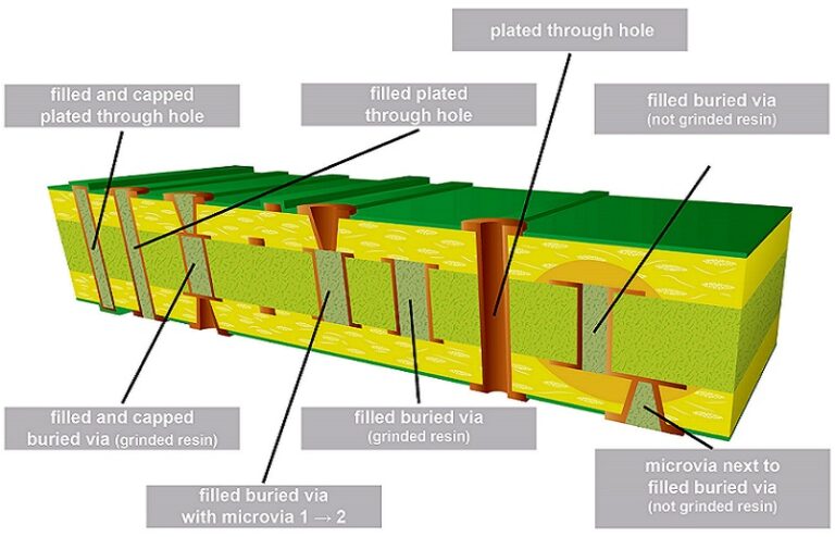
Blind and Buried Vias in HDI PCB
Blind and buried vias form the core structural elements of high-density interconnect (HDI) PCB systems, enabling targeted layer-to-layer electrical connections…

Blind and buried vias form the core structural elements of high-density interconnect (HDI) PCB systems, enabling targeted layer-to-layer electrical connections…
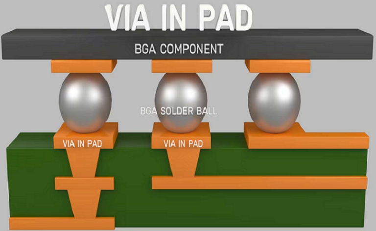
Via-in-Pad (VIPPO) technology places plated microvias directly within component pads in HDI PCBs, enabling higher routing density, shorter electrical paths,…
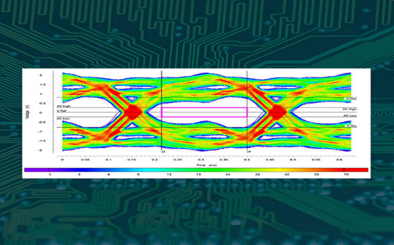
Signal integrity challenges in HDI PCBs arise from miniaturized geometries, high-density routing, and high-speed signaling, creating issues including impedance mismatch,…
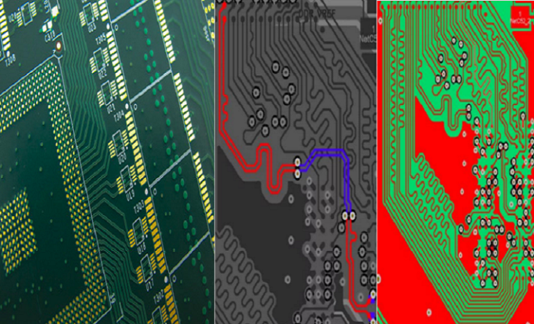
Impedance control in HDI PCB design ensures consistent characteristic impedance across transmission lines by optimizing layer stackup, trace geometry, microvia…
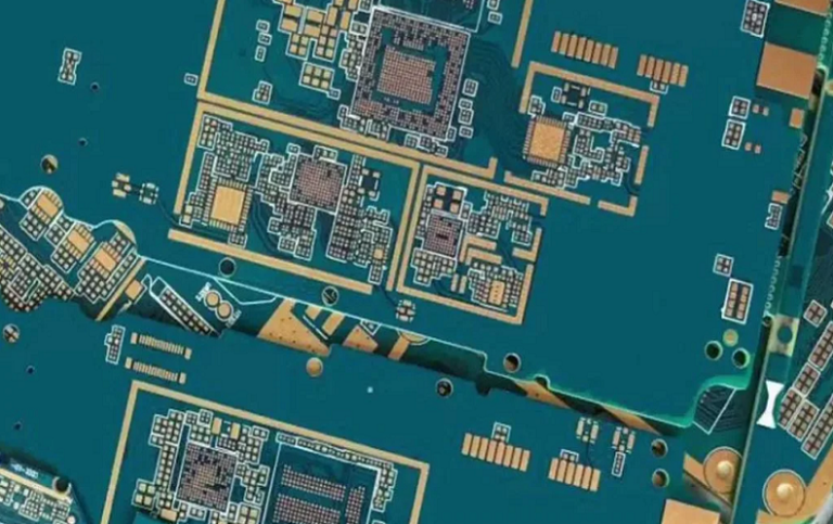
Top global HDI PCB manufacturers deliver high-density interconnect solutions with advanced microvia technology, sequential lamination, fine-line imaging, and controlled impedance…
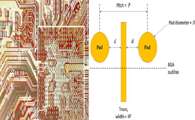
BGA routing in HDI PCBs delivers optimized fanout and escape structures for fine‑pitch semiconductor packages, supporting reliable high‑density interconnection, impedance…
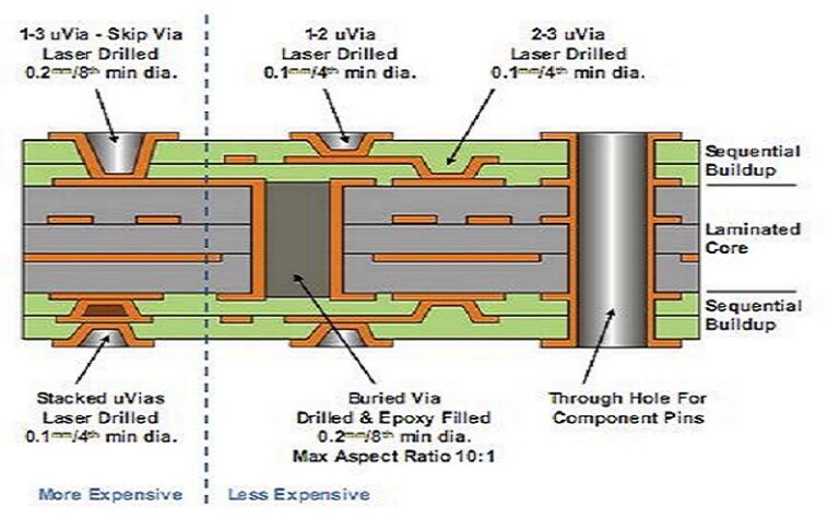
HDI PCB stackup design for high-speed signals provides a disciplined, manufacturing-ready approach to layer arrangement, dielectric selection, microvia configuration, and…
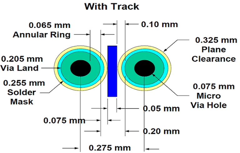
HDI PCB design guidelines define a strict set of dimension rules, material selections, stackup strategies, and manufacturing constraints aligned with…
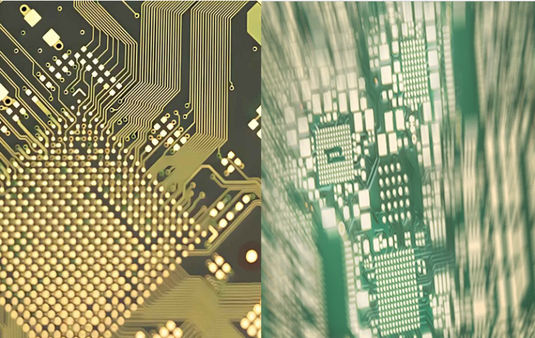
Microvia HDI PCB represents the foundation of modern high-density interconnect technology, using laser-drilled vias ≤150μm with aspect ratio ≤1:1, sequential…