







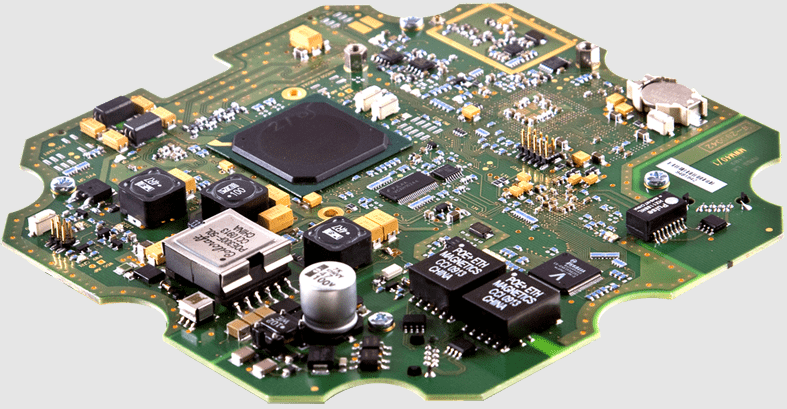
Turnkey PCB assembly provides a complete electronics manufacturing solution where one manufacturing partner manages the entire process from PCB fabrication, component procurement, circuit board assembly, inspection, testing, and final delivery. Compared with partial assembly models, turnkey PCB assembly reduces supply chain complexity, improves production control, and shortens product development cycles.
A professional turnkey PCB assembly service combines PCB manufacturing capabilities, electronic component sourcing, SMT placement, through-hole assembly, inspection, and functional testing into one integrated workflow. The process normally follows IPC-2221 design guidelines, IPC-6012 PCB qualification requirements, and IPC-A-610 electronic assembly acceptance standards.
For engineers developing industrial equipment, medical electronics, automotive controllers, communication systems, and HDI PCB products, turnkey manufacturing provides better control over quality, traceability, and production efficiency.
A complete turnkey PCB assembly workflow includes:
- PCB fabrication and material selection
- Component purchasing and verification
- Surface Mount Technology (SMT)
- Through-Hole Technology (THT)
- Solder paste printing
- Pick-and-place assembly
- Reflow soldering
- Automated Optical Inspection (AOI)
- X-ray inspection
- Electrical testing
- Functional validation
What Is Turnkey PCB Assembly?
Complete Manufacturing Integration
Turnkey PCB assembly means the manufacturer manages all production activities instead of requiring customers to provide separate PCB boards, components, or assembly resources.
The turnkey model typically covers:
- Engineering review
- PCB design verification
- PCB fabrication
- Bill of Materials (BOM) management
- Component procurement
- PCB assembly
- Testing
- Packaging
The main value is process integration.
A traditional PCB assembly model may require:
- One supplier for PCB fabrication
- Another supplier for components
- Another supplier for assembly
- Separate quality management
A turnkey PCB assembly supplier combines these steps into one controlled manufacturing system.
PCB Assembly vs Turnkey PCB Assembly
| Item | Traditional PCB Assembly | Turnkey PCB Assembly |
|---|---|---|
| PCB sourcing | Customer managed | Manufacturer managed |
| Component purchasing | Customer responsibility | Supplier responsibility |
| Supply chain control | Multiple suppliers | Single supplier |
| Engineering support | Limited | Integrated |
| Production tracking | More complex | Centralized |
For product developers, turnkey manufacturing reduces coordination time and improves production visibility.
PCB vs PCBA Difference
A PCB is the bare circuit board containing:
- Copper traces
- Dielectric layers
- Pads
- Vias
A PCBA is the finished assembly after components are mounted.
The relationship:
PCB → Component placement → Soldering → Testing → PCBA
A printed circuit board assembly includes:
- PCB substrate
- Electronic components
- Solder joints
- Connectors
- Mechanical elements
PCB Fabrication
PCB Material Selection
The first stage of turnkey PCB assembly is producing the bare PCB.
Common PCB materials include:
- FR-4 fiberglass laminate
- High Tg materials
- Polyimide materials
- High-frequency laminates
Typical PCB parameters:
| Parameter | Typical Range |
|---|---|
| Board thickness | 0.6 mm–3.2 mm |
| Copper thickness | 1 oz–3 oz |
| Minimum trace width | 3 mil–5 mil |
| Minimum spacing | 3 mil–5 mil |
| Via diameter | 0.15 mm–0.30 mm |
| Impedance tolerance | ±10% |
For advanced HDI PCB applications:
- Laser microvias may be 75–150 µm
- Line spacing may reach 2.5/2.5 mil
- Sequential lamination structures may use 1+N+1 or 2+N+2 configurations
PCB Fabrication Process
The PCB fabrication process includes:
- Inner layer imaging
- Copper etching
- Layer lamination
- Mechanical drilling
- Laser drilling for HDI structures
- Copper plating
- Solder mask application
- Surface finishing
Common surface finishes include:
- ENIG
- HASL
- Immersion silver
- OSP
ENIG is widely used for high-reliability printed circuit assembly because it provides:
- Flat solder surface
- Good corrosion resistance
- Suitable fine-pitch component assembly
Manufacturing Quality Control
PCB fabrication inspection includes:
- AOI inspection
- Layer alignment verification
- Copper thickness measurement
- Impedance testing
- Micro-section analysis
Typical factory controls:
- Layer registration: ±50–75 µm
- Copper thickness variation: controlled within manufacturing limits
- Electrical testing: 100% open/short test
Component Procurement
BOM Management
Component procurement is a critical part of turnkey PCB assembly.
The manufacturer manages:
- Bill of Materials review
- Part number verification
- Supplier qualification
- Inventory planning
- Obsolescence control
A complete BOM includes:
- Manufacturer part number
- Quantity
- Package type
- Electrical specification
- Approved alternatives
Component Verification
Incoming components require inspection before assembly.
Quality checks include:
- Part number confirmation
- Label verification
- Moisture sensitivity level (MSL) checking
- Packaging inspection
Common package types:
- 0201
- 0402
- 0603
- QFN
- BGA
- CSP
For advanced circuit card assembly, BGA inspection normally requires X-ray analysis because solder joints are hidden underneath the package.
Supply Chain Advantages
Turnkey sourcing provides:
- Reduced procurement workload
- Better component traceability
- Faster production scheduling
Comparison:
| Feature | Customer-Supplied Components | Turnkey Component Sourcing |
|---|---|---|
| Purchasing control | Customer | Manufacturer |
| Inventory management | Customer | Manufacturer |
| Supplier qualification | Customer | Manufacturer |
| Production flexibility | Medium | High |
Assembly Process
SMT Assembly
Surface Mount Technology is the primary method used in modern pcb assembly.
The SMT process includes:
- Solder paste printing
- Component placement
- Reflow soldering
- Inspection
Typical SMT parameters:
- Solder paste thickness: 80–150 µm
- Placement accuracy: ±25–50 µm
- Reflow peak temperature: 235°C–250°C
Solder Paste Printing
The process starts with applying solder paste onto PCB pads.
Steps:
- Stainless steel stencil alignment
- Solder paste application
- Paste inspection
Typical stencil thickness:
- 0.08 mm–0.15 mm
The goal is:
- Correct solder volume
- Uniform deposition
- Reduced solder defects
Common problems include:
- Insufficient solder
- Excess solder
- Bridging
Pick-and-Place Assembly
Automated machines place components onto solder paste.
Process:
- Feeders supply components
- Vision system identifies orientation
- Placement head installs components
High-speed machines can place:
- Tens of thousands of components per hour
Placement accuracy:
- Approximately ±25 µm for advanced equipment
Reflow Soldering
During reflow:
- PCB enters heating zones
- Solder paste melts
- Components bond to pads
- Cooling solidifies solder joints
Typical profile:
- Preheat: 150°C–180°C
- Soak: 180°C–220°C
- Peak: 235°C–250°C
- Cooling rate: controlled to prevent thermal stress
Testing and Inspection
Automated Inspection
Quality inspection is essential for reliable printed circuit board assembly.
Inspection methods include:
AOI Inspection
Automated Optical Inspection checks:
- Component presence
- Polarity
- Solder quality
- Placement accuracy
X-Ray Inspection
X-ray inspection is used for:
- BGA packages
- QFN components
- Hidden solder joints
Typical inspection focuses:
- Voids
- Opens
- Solder bridging
Electrical Testing
Electrical testing verifies circuit performance.
Methods include:
- Flying probe testing
- In-circuit testing (ICT)
- Functional testing
Testing verifies:
- Continuity
- Resistance
- Voltage behavior
- System operation
Quality Control Standards
Professional turnkey PCB assembly follows:
- IPC-A-610 acceptance criteria
- IPC-J-STD-001 soldering requirements
- ISO 9001 quality management systems
Quality control checkpoints:
| Production Stage | Inspection Method |
|---|---|
| PCB fabrication | AOI, electrical test |
| Incoming components | Verification inspection |
| SMT placement | AOI |
| BGA assembly | X-ray |
| Final assembly | Functional test |
Real Factory Case Study: Industrial HDI PCB Assembly
A customer required a compact industrial controller with high reliability.
Product requirements:
- 12-layer HDI PCB
- 2+N+2 stack-up
- FR-4 high Tg material
- 100 Ω differential impedance
- BGA processor package
Initial manufacturing challenge:
- Fine-pitch BGA solder defects
- Limited assembly space
- High component density
Production parameters:
- Minimum trace width: 3 mil
- Microvia diameter: 100 µm
- Surface finish: ENIG
- Component package: 0201 and BGA
Root causes:
- Excess solder paste volume
- Incorrect stencil opening design
Manufacturing improvements:
- Optimized stencil thickness from 0.15 mm to 0.12 mm
- Adjusted paste volume control
- Added X-ray inspection after reflow
Final results:
- Reduced solder defects
- Improved first-pass yield
- Increased production consistency
Common Design Errors
Incorrect PCB Design for Assembly
Common issues:
- Components too close together
- Incorrect pad dimensions
- Missing thermal relief design
Solutions:
- Early DFM review
- Manufacturer collaboration
- IPC guideline verification
Poor Component Selection
Problems include:
- Obsolete components
- Long lead-time parts
- Incorrect package selection
Factory engineers evaluate:
- Availability
- Alternative parts
- Assembly compatibility
Ignoring Testing Requirements
Designs should consider:
- Test points
- Programming interfaces
- Functional validation requirements
Without proper testing access, production troubleshooting becomes difficult.
FAQ
Q1: What is turnkey PCB assembly?
Turnkey PCB assembly is a complete manufacturing service where one supplier manages PCB fabrication, component procurement, assembly, inspection, and testing.
Q2: What is the difference between PCB and PCBA?
A PCB is the bare circuit board, while a PCBA is the finished product after electronic components are assembled and tested.
Q3: When should engineers choose turnkey PCB assembly services?
Turnkey manufacturing is suitable for products requiring supply chain control, consistent quality, faster production, and integrated engineering support.
Q4: Can turnkey PCB assembly support HDI PCB production?
Yes. Advanced turnkey suppliers can support HDI PCB manufacturing with microvias, fine-pitch components, controlled impedance, and high-density assembly processes.

![Understanding PCB Costs & Pricing [Your Complete Guide]](https://hdicircuitboard.com/wp-content/uploads/elementor/thumbs/Understanding-PCB-Costs-Pricing-Your-Complete-Guide-qzzhe6mcaxuolkux3xalfktgavumi9y1aqfbs9bpv4.webp "Understanding PCB Costs & Pricing [Your Complete Guide]")