
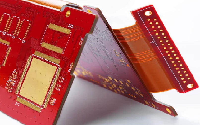
High speed flex PCB engineering integrates high-frequency signal integrity, dynamic mechanical flexibility, and precision fabrication constraints to mitigate impedance fluctuation, crosstalk, and bend-induced electrical degradation. This factory-focused guide delivers quantified design parameters, layer configuration rules, routing methodologies, and mechanical control standards for flexible printed circuit board and rigid flex PCB high-speed applications aligned with IPC-2221 and IPC-6012 industry specifications.
Learn more about: Flexible PCB Impedance Control Guide
Key High-Speed Flex PCB Design Tips
Balancing Electrical and Mechanical Performance
- High-frequency signals above 1GHz require consistent dielectric integrity across flexible zones to limit insertion loss below 0.8dB per 100mm
- Mechanical flex stress creates micro-copper fractures that raise trace resistance by 12–18% in repeated bend cycles
- Symmetrical layer construction eliminates thermal expansion mismatch, maintaining Dk stability at 3.1–3.5 across -40°C to 125°C
- All high-speed design modifications must satisfy IPC-2223 flexible circuit durability classifications for long-term production viability
Manufacturing Alignment for High-Velocity Signals
- Etch factor calibration set to 1.6–1.9 for 12μm and 18μm rolled annealed copper to preserve controlled trace geometry
- Panelization gaps of 2.0mm minimum between rigid-flex transition zones to reduce lamination pressure distortion
- Pre-production stack-up validation verifies adhesive flow thickness at 15μm ±3μm, preventing uneven dielectric compression
- High-speed test coupons embedded on each production panel for TDR impedance validation per IPC-TM-650 2.5.5.7
Stack-Up and Material Selection
Symmetrical Layer Stack-Up Architecture
- 2-layer high speed flex PCB: Signal / Ground cross-hatched plane, 75μm polyimide core with 12μm acrylic adhesive
- 4-layer rigid flex PCB: Signal / Ground / Power / Signal, 50μm core dielectrics with balanced bonding film layers
- 6-layer premium high-speed structure: Signal / Ground / Signal / Power / Ground / Signal for crosstalk reduction up to 35%
- Asymmetrical stack-up restricted entirely in high-speed designs, as uneven layer tension causes 6–9% impedance drift during bending
Low-Loss Dielectric and Copper Grading
- High-speed polyimide dielectric with Dk 3.2 ±0.08 and loss tangent 0.003 @10GHz for signal stability
- No-adhesive flex substrates specified for 5GHz+ circuits to remove variable adhesive Dk interference
- Rolled annealed copper with 0.3% minimum elongation mandatory for dynamic flex zones; electrodeposited copper limited to static sections
- Coverlay material selected with matched Dk values to avoid secondary capacitive loading on exposed high-speed traces
Learn more about: Flexible PCB Layer Stackup: Complete Design Guide
Controlled Impedance Management
Impedance Parameter Calibration for Flex Zones
- Standard target impedance values: 50Ω single-ended, 90Ω coplanar, 100Ω differential pair with ±5% tolerance (IPC Class 2)
- Dielectric thickness tolerance held to ±4μm across flexible regions to restrict impedance variation under bending
- Cross-hatched ground planes increase nominal impedance by 4–7%, requiring trace width reduction of 0.03–0.05mm during layout
- High-speed flex impedance calculations incorporate bend compression factors that reduce effective dielectric height by 2–3% under repeated flexing
Simulation and Production Validation Rules
- 2D field solver simulation completed at operational bend states to capture loaded impedance performance
- Thermal impedance sweep from 0°C to 105°C identifies high-speed signal deviation in temperature-variable devices
- Production batch testing requires 100% inspection of differential high-speed routes and 15% sampling for single-ended lines
- Post-fabrication reflow cycling verifies impedance retention after 3x standard soldering thermal exposure
Routing Practices in Flex Zones
Stagger Traces Layout Principles
- Staggered trace routing offsets adjacent layer high-speed lines by 0.25mm minimum to eliminate vertical crosstalk coupling
- Offset spacing increased to 0.35mm for dense 4-layer flex designs with signal frequencies exceeding 3GHz
- Parallel vertical trace alignment prohibited within flexible zones, as overlapping routing creates 22% higher electromagnetic interference
- Stagger patterns repeated uniformly across continuous bend areas to distribute mechanical stress evenly across copper traces
Curved Traces and Perpendicular Bends Implementation
- Curved trace arcs with 0.2mm minimum radius replace sharp transitions to limit high-speed signal reflection below 0.05dB
- Perpendicular bends aligned transverse to the primary flex axis to reduce copper tensile stress during compression cycles
- 45° transitional routing used at rigid-flex boundaries to gradualize mechanical load transfer between rigid and flexible substrates
- Trace width maintained consistently through curved segments; tapered routing restricted to low-speed power lines only
Via and Land Pattern Design
High-Speed Via Restrictions in Flexible Areas
- Through-hole vias fully excluded from dynamic bend zones; minimum clearance of 2.5mm from repeated flex regions
- Microvia diameters capped at 0.15mm for high-speed rigid flex PCB designs with 0.10mm annular ring dimensions
- Via anti-pad clearance set to 0.3mm minimum to reduce parasitic capacitance on high-speed signal transitions
- Multiple small stitching vias at 0.5mm intervals strengthen ground plane continuity without introducing high-speed signal noise
Land Pattern Stress Reduction Modifications
- Teardrop land transitions applied to all high-speed component pads within 3mm of rigid-flex borders
- Elongated oval land patterns reduce corner stress concentration by 40% compared to square rectangular pads
- Solder mask defined lands specified for flex-mounted components to eliminate solder fillet cracking during minor substrate movement
- High-speed differential pair lands matched for identical geometry to preserve propagation delay balance
Stiffeners and Supporting Structures
Stiffener Material and Boundary Design
- 0.10mm polyimide stiffeners for localized component support on high speed flex PCB without restricting distant bend motion
- FR-4 stiffeners limited to static mounting zones; rigid-flex transition edges rounded with 0.5mm radius to prevent substrate tearing
- Stiffener adhesive coverage restricted to 90% of bonded area to allow minor flex substrate expansion and contraction
- High-speed connector regions reinforced with double-layer stiffeners to maintain flatness and consistent contact impedance
Transition Zone Reinforcement Methods
- Graduated layer thinning at rigid-flex junctions creates gradual mechanical transition, lowering stress riser formation
- Reinforced bonding film with 20μm thickness applied at transition zones to enhance tear resistance for high-density routing
- Cutback rigid layer edges offset 1.0mm from active high-speed traces to avoid dielectric crimping during flex movement
- Factory lamination pressure adjusted to 185 psi in transition zones to prevent resin squeeze-out and dielectric thinning
Learn more about : Flexible PCB Design Guidelines
Grounding and Shielding
Continuous Ground Plane Architecture
- Cross-hatched ground planes implemented across all flexible high-speed sections with 55–60% open area for improved bend fatigue
- Solid ground planes permitted only in static rigid flex segments to preserve shielding performance without mechanical failure
- Ground plane segmentation blocked in high-speed zones; any necessary gaps limited to 0.15mm maximum width
- Isolated ground stitching vias placed every 4mm along high-speed channel borders to contain stray high-frequency radiation
Flexible Shielding Film Integration
- 12μm copper shielding laminates bonded to outer flex layers for 25dB noise attenuation at 2.4GHz high-speed bands
- Shield layer isolation gaps maintained at 0.2mm from high-speed signal edges to prevent capacitive signal loading
- Shield grounding points limited to single-ended connection per continuous flex segment to avoid ground loop high-speed interference
- Thin conductive adhesive shielding materials selected to retain minimum bend radius requirements for dynamic applications
Mechanical Considerations for High-Speed Reliability
Bend Radius Quantified Specifications
- Static single-install bend radius maintained at 6x total flexible PCB thickness, limiting impedance shift to under 3%
- Dynamic cyclic bending requires 10x substrate minimum radius to prevent trace cracking across 100,000 operational cycles
- High-speed differential pairs require 12x thickness bend radius due to heightened sensitivity to asymmetric stress distortion
- Inner layer flex traces positioned closer to neutral bend axis to reduce tensile and compressive load differentials
Coverlay Usage and Protective Design
- 25μm polyimide coverlay standardized for high speed flex PCB, with laser-defined openings for precision high-speed pad access
- Coverlay overlap margins of 0.8mm minimum over bend zone edges to seal adhesive layers and block environmental moisture ingress
- Partial coverlay removal restricted to non-critical low-speed regions; continuous coverlay coverage preserves consistent dielectric loading
- Cold-pressed coverlay lamination process eliminates micro-voids that cause high-speed signal scattering at frequencies above 5GHz
Core Parameter Comparative Analysis
Solid Ground Plane vs Cross-Hatched Ground Plane
| Parameter | Solid Ground Plane | Cross-Hatched Ground Plane |
|---|---|---|
| High-Speed Shielding | 35dB @5GHz | 24dB @5GHz |
| Dynamic Bend Cycle Life | 15,000 cycles | 110,000 cycles |
| Flex Zone Impedance Shift | 7–9% under bend | 2–4% under bend |
| Dielectric Heat Retention | Elevated thermal buildup | Improved heat dissipation |
| High-Speed Crosstalk Control | Superior isolation | Moderate controlled coupling |
Curved Traces vs Perpendicular Sharp Bends
| Feature | Curved Traces | Perpendicular Sharp Bends |
|---|---|---|
| High-Speed Signal Loss | ≤0.04dB per bend | 0.18dB per bend |
| Copper Stress Fatigue Risk | Low localized tension | High corner fracture rate |
| Impedance Continuity | Stable 48–52Ω | Fluctuates 43–57Ω |
| Layout Density Efficiency | Moderate footprint | Compact constrained routing |
| Fabrication Etch Consistency | Uniform trace geometry | Uneven corner etching wear |
Verified High-Speed Flex PCB Technical Parameters
High-Speed Routing and Fabrication Metrics
- Minimum high-speed trace width: 0.12mm for 18μm RA copper, 0.10mm for 12μm thin copper flex circuits
- Differential pair spacing: 0.18mm fixed gap for 100Ω high-speed channels with length matching tolerance ±0.08mm
- Flexible substrate total thickness: 0.12mm to 0.20mm for high-speed dynamic applications
- Rigid flex PCB transition edge tolerance: ±0.05mm laser cutting precision to reduce mechanical stress points
- High-speed line spacing follows 3W design rule with 0.36mm minimum separation for 0.12mm signal traces
Quality Control and Compliance Standards
- IPC-6013 Class 3 compliance mandated for automotive and industrial high-speed flexible circuit assemblies
- 10GHz bandwidth TDR testing conducted on all controlled impedance high-speed routes
- Micro-section analysis sampling at 5% production volume validates layer dielectric thickness and adhesive uniformity
- Environmental cycling testing (-40°C to 125°C, 500 cycles) confirms high-speed signal stability through thermal expansion shifts
High-Speed Flex PCB Case Study
Project Core Specifications
- Application: Industrial high-definition data transmission rigid flex PCB
- Layer Configuration: 4-layer symmetrical high speed flex PCB with 0.15mm flexible core
- Key Requirements: 100Ω differential high-speed lanes, 5GHz bandwidth, 50,000 dynamic bend cycles
- Original Design Setup: Solid inner ground planes, perpendicular right-angle bends, standard 3x thickness bend radius
Documented Production and Performance Issues
- Measured 11% impedance deviation in repeated flex zones causing data packet loss during physical movement
- Right-angle bend trace micro-cracking observed after 12,000 flex cycles, increasing differential pair skew to 1.2ps/cm
- Solid ground plane layer delamination initiated at rigid-flex transition edges after thermal reflow exposure
- Inconsistent coverlay adhesive thickness created variable dielectric loading leading to 0.7dB insertion loss fluctuation
Targeted Engineering Design Revisions
- Replaced solid ground layers with optimized 0.5mm grid cross-hatched planes for balanced flexibility and shielding
- Redesigned all high-speed routing with 0.2mm curved arc bends and staggered trace offset layer alignment
- Increased dynamic bend radius to 10x substrate thickness and implemented perpendicular flex-axis routing
- Upgraded to low-loss no-adhesive polyimide dielectric and standardized 25μm laser-cut coverlay application
- Added graduated rigid-flex transition layer thinning and reinforced bonding film at boundary zones
Final Measurable Performance Improvements
- Differential impedance variation reduced to ±3.8% with consistent 98.7Ω average across full flex motion range
- Functional bend cycle lifespan extended to 65,000 cycles with zero high-speed trace fracture or resistance drift
- High-speed channel insertion loss stabilized at 0.32dB per 100mm with minimal fluctuation through thermal cycling
- Production yield increased from 76% to 94% through reduced rigid-flex delamination and etching-related high-speed defects
Common High-Speed Flex PCB Design Errors
- Overusing solid continuous ground planes across flexible zones, creating concentrated stress that fractures copper layers in dynamic bending
- Routing high-speed differential pairs parallel to primary bend axes, generating asymmetric tension and critical timing skew deviation
- Placing high-speed vias and component lands within 2mm of rigid-flex transition borders, triggering pad lifting and dielectric crimping
- Ignoring coverlay dielectric loading effects, resulting in miscalculated impedance values that fail post-fabrication high-speed testing
- Applying inconsistent trace width through curved flex segments, creating abrupt impedance discontinuities for high-frequency signal flow
- Skipping staggered interlayer routing, leading to vertical crosstalk that degrades 3GHz+ high-speed data transmission integrity
- Specifying undersized bend radii for multi-layer rigid flex PCB, accelerating adhesive separation and layered substrate fatigue
- Neglecting ground stitching via placement along high-speed flex boundaries, allowing unfiltered high-frequency noise coupling
High Speed Flex PCB Design FAQ
Q: What core material properties directly impact high-speed performance in flexible printed circuit board designs?
A: Dielectric Dk and loss tangent stability across temperature and bend states serve as primary performance factors, paired with rolled annealed copper ductility and uniform adhesive layer thickness. Low-loss polyimide substrates with fixed 3.2 Dk ratings minimize high-speed signal attenuation, while balanced layer stack-up prevents mechanical distortion that disrupts impedance control.
Q: How do curved traces improve high-speed reliability compared to angular bends in bendable circuit board layouts?
A: Curved trace routing eliminates sharp impedance discontinuities that reflect high-frequency signals, reducing insertion loss by 75% in flex zones. Rounded arc routing distributes mechanical tension evenly across copper pathways, lowering micro-fracture formation risk and maintaining consistent electrical performance through repeated flexible PCB movement cycles.
Q: What critical differences separate solid and cross-hatched ground planes for high-speed rigid flex PCB integration?
A: Solid ground planes deliver superior high-frequency shielding but suffer poor flex durability and significant impedance drift under bending. Cross-hatched structures enhance mechanical flexibility for dynamic applications and stabilize bend-induced impedance shifts, with marginal high-speed noise reduction trade-offs manageable through strategic shielding film and stitching via implementation.
Q: What bend radius standards should engineers follow for multi-layer high speed flex PCB dynamic and static installations?
A: Static fixed flex applications require a minimum 6x overall substrate thickness radius, while continuous dynamic bending demands 10x thickness for general high-speed circuits and 12x thickness for sensitive differential high-speed pairs. All bend radius calculations adhere to IPC-2223 flexible circuit design specifications to sustain long-term signal integrity and mechanical durability.
If you need professional flexible circuit board design support or quotation, our team provides free DFM check and fast turnaround.


