







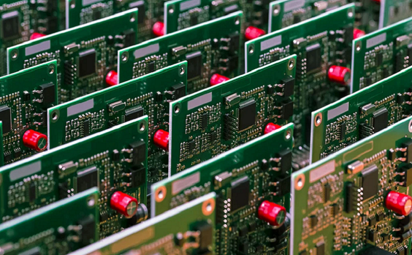
HDI PCB Assembly involves advanced manufacturing technologies that enable smaller electronic products, faster signal transmission, and improved power distribution. However, high-density designs introduce more complex assembly risks compared with traditional multilayer PCBs. The most common HDI PCB Assembly Risks include solder bridging and shorts, component misalignment, microvia reliability failures, delamination, voids, and thermal stress cracking.
A successful HDI (High-Density Interconnect) PCB assembly process requires close control of PCB fabrication, material selection, component placement, solder paste printing, reflow soldering, and inspection. Typical high-performance HDI circuit boards use structures such as 1+N+1, 2+N+2, or 3+N+3 sequential lamination, with laser microvias ranging from 75μm to 150μm, line width and spacing from 3/3 mil to 5/5 mil, and controlled impedance requirements of 50Ω ±5% or ±10%.
Professional HDI PCB manufacturers reduce assembly failures through Design for Manufacturability (DFM), microvia plugging, precise temperature control, advanced inspection methods, and compliance with IPC standards including IPC-2221, IPC-6012, IPC-A-610, and IPC-J-STD-001.
Why HDI Matters
Smaller Size and Higher Density
HDI technology allows engineers to achieve higher circuit density within smaller PCB dimensions. Traditional multilayer PCB designs rely mainly on through-hole vias, while HDI PCB fabrication uses laser-drilled microvias, blind vias, buried vias, and via-in-pad structures.
The main advantages include:
- Reduced PCB size
- More routing channels
- Smaller component footprint
- Higher layer utilization
- Improved electrical performance
For example, a standard 8-layer PCB may require a board area of 100mm × 80mm for complex routing, while an HDI PCB with 2+N+2 structure may reduce the required area by 30%-50%.
Faster Signals and Better Power
High-speed electronic systems require shorter signal paths and controlled return current paths. HDI circuit boards improve signal integrity by reducing via inductance and minimizing unnecessary layer transitions.
Typical high-speed HDI applications include:
- AI hardware
- Automotive radar modules
- Medical imaging devices
- 5G communication equipment
- Industrial control systems
Common electrical requirements:
- Differential impedance: 90Ω-100Ω
- Single-ended impedance: 50Ω
- Impedance tolerance: ±5% for advanced applications
- Low-loss materials: Panasonic Megtron, Rogers, ITEQ high-speed laminates
Better Power Distribution
HDI designs improve power delivery by providing more efficient power and ground connections.
Advantages include:
- Shorter power paths
- Lower voltage drop
- Reduced electromagnetic interference
- Better thermal performance
Microvia structures allow engineers to place power connections closer to BGA pads, improving current distribution for high-density semiconductor packages.
HDI PCB Assembly Steps
Solder Paste Printing
Solder paste printing is one of the most critical HDI PCB assembly steps because fine-pitch components require extremely accurate paste volume control.
The process includes:
- PCB alignment with stencil
- Solder paste application
- Stencil separation
- SPI inspection
Typical manufacturing parameters:
| Parameter | Typical Value |
|---|---|
| Stencil thickness | 0.10mm-0.15mm |
| Fine-pitch BGA | 0.35mm-0.5mm pitch |
| SPI accuracy | ±25μm |
| Solder paste type | SAC305 lead-free |
Common risks:
- Excess solder volume
- Insufficient solder volume
- Paste contamination
- Poor aperture design
For HDI PCB Assembly, solder paste control is more challenging because micro-BGA and via-in-pad designs have smaller pad geometries.
Component Placement
High-density components require precise placement equipment.
Modern SMT machines typically provide:
- Placement accuracy: ±25μm to ±50μm
- High-speed placement capability
- Automatic optical alignment
Important factors include:
- Component package size
- Fiducial mark design
- PCB warpage
- Placement pressure
Common HDI component packages:
- 0201 passive components
- QFN
- CSP
- WLCSP
- Fine-pitch BGA
Incorrect placement can cause:
- Open solder joints
- Short circuits
- Component shifting
- Reliability failures
Reflow Soldering
Reflow soldering creates permanent electrical connections between components and PCB pads.
HDI PCB assembly requires precise temperature control because thin multilayer structures are sensitive to thermal stress.
Typical lead-free reflow profile:
| Stage | Temperature |
|---|---|
| Preheat | 150°C-180°C |
| Soak | 180°C-220°C |
| Peak | 235°C-250°C |
| Cooling rate | Less than 4°C/sec |
Poor temperature control may cause:
- PCB warpage
- Delamination
- Pad lifting
- Solder cracking
Inspection
HDI PCB assembly requires multiple inspection stages.
Quality control includes:
- SPI solder paste inspection
- AOI inspection
- X-ray inspection
- Electrical testing
- Functional testing
Inspection targets:
- Microvia connection
- BGA solder joints
- Solder volume
- Component alignment
- Surface defects
For advanced HDI PCB prototypes, X-ray inspection is often required because hidden solder joints cannot be verified visually.
Assembly Challenges
Solder Bridging and Shorts
Solder bridging occurs when excessive solder connects two adjacent pads.
Common causes:
- Incorrect stencil opening
- Excess solder paste
- Small component spacing
- Poor PCB pad design
Typical failure areas:
- 0.4mm BGA
- 0.35mm CSP packages
- Fine-pitch connectors
Prevention methods:
- Optimize stencil aperture
- Control solder paste thickness
- Use SPI inspection
- Improve pad geometry
For HDI circuit boards, solder bridging risk increases because routing density forces smaller component spacing.
Misalignment and Shifting
Component misalignment occurs when components move during placement or reflow.
Main causes:
- Incorrect placement parameters
- PCB warpage
- Uneven solder paste distribution
- Excessive reflow vibration
Typical tolerance:
- SMT placement accuracy: ±25μm-50μm
- Fine-pitch component alignment requirement: within ±50μm
Solutions include:
- Better fiducial design
- Accurate PCB panel positioning
- Optimized reflow profile
Delamination and Voids
Delamination happens when layers separate inside the PCB structure.
For HDI PCB fabrication, common causes include:
- Poor resin filling
- Insufficient lamination pressure
- Material mismatch
- Excess moisture
Voids inside microvias or resin-filled vias can reduce reliability.
Typical HDI requirements:
- Microvia diameter: 75μm-150μm
- Aspect ratio: approximately 0.75:1 or lower for reliable filling
- Via filling quality: no significant internal voids
Thermal Stress and Cracking
Temperature Control During Assembly
HDI PCB assembly uses thinner dielectric layers and complex sequential lamination structures, making thermal management critical.
Thermal stress can cause:
- Copper cracking
- Microvia fracture
- Resin cracking
- Solder joint fatigue
Common causes:
- Excessive reflow cycles
- Incorrect heating rate
- Material expansion mismatch
A typical PCB assembly limit:
- Maximum reflow cycles: 3-6 cycles depending on material system
Microvia Reliability
Microvias experience mechanical stress during thermal cycling.
Failure mechanisms include:
- Copper barrel cracking
- Interface separation
- Bottom microvia failure
Improvement methods:
- Proper laser drilling parameters
- Optimized copper plating
- Reliable microvia plugging
How to Prevent These Risks
Design for Manufacturability (DFM)
DFM is one of the most effective methods to reduce HDI PCB Assembly Risks before production.
Engineers should review:
- Component spacing
- Pad design
- Via structure
- Stackup
- Impedance requirements
- Thermal design
Recommended HDI design parameters:
| Item | Typical Capability |
|---|---|
| Line width/space | 3/3 mil – 5/5 mil |
| Microvia size | 75μm-150μm |
| BGA pitch | 0.35mm-0.8mm |
| Layer count | 6-20 layers |
| Impedance control | ±5%-10% |
Plug Your Vias
Microvia plugging is essential for reliable HDI assembly.
Via plugging methods include:
- Resin filled vias
- Copper filled vias
- Via-in-pad plated over (VIPPO)
Benefits:
- Prevent solder leakage
- Improve BGA reliability
- Increase routing density
- Improve thermal performance
Traditional vias and HDI microvias have different requirements:
| Feature | Traditional Via | HDI Microvia |
|---|---|---|
| Drilling Method | Mechanical drilling | Laser drilling |
| Diameter | 0.15mm-0.3mm | 0.075mm-0.15mm |
| Application | Standard PCB | High-density PCB |
| Manufacturing Complexity | Lower | Higher |
HDI PCB Assembly Risks vs Traditional PCB Assembly
| Category | Traditional PCB Assembly | HDI PCB Assembly |
|---|---|---|
| Via Technology | Through-hole vias | Microvias, blind vias, buried vias |
| Routing Density | Medium | Very high |
| Assembly Difficulty | Standard SMT | Fine-pitch SMT and BGA |
| Inspection Requirement | AOI mainly | AOI + X-ray + advanced testing |
| Thermal Risk | Lower | Higher |
Real Factory Case Study
10-Layer HDI PCB Assembly for Communication Equipment
A customer required a compact communication module using HDI PCB technology.
Specifications:
- Layer count: 10 layers
- HDI structure: 2+N+2
- Material: High Tg FR-4
- Board thickness: 1.2mm
- Minimum line width/spacing: 4/4 mil
- Microvia diameter: 100μm
- BGA pitch: 0.4mm
- Controlled impedance: 50Ω ±5%
Initial assembly issue:
During first prototype assembly:
- BGA solder joints showed inconsistent connection
- Several microvias failed electrical testing
- Resin-filled vias contained small voids
Root causes:
- Insufficient microvia plugging quality
- Excess solder paste volume
- Reflow peak temperature variation
Manufacturing improvements:
- Adjusted via filling parameters
- Optimized stencil aperture by 8%
- Improved reflow thermal profile
- Added X-ray inspection after assembly
Final result:
- Passed electrical testing
- Passed thermal cycling evaluation
- Achieved stable prototype validation
Common Design Errors From Production Perspective
Incorrect Via-in-Pad Design
Problem:
Unfilled vias under BGA pads may absorb solder during reflow.
Result:
- Open solder joints
- BGA connection failure
Solution:
Use resin-filled and copper-capped via structures.
Ignoring Stackup Design
Problem:
Poor layer planning creates impedance variation and signal integrity problems.
Solution:
Control:
- Dielectric thickness
- Copper thickness
- Material Dk value
- Reference plane structure
Insufficient Thermal Planning
Problem:
High-power components create localized heating.
Solution:
Use:
- Thermal vias
- Copper areas
- Proper power plane design
FAQ
Q1: What are the biggest HDI PCB Assembly Risks?
Answer:
The biggest risks include solder bridging, component misalignment, microvia failure, delamination, voids, and thermal cracking. These risks increase as HDI designs use smaller features, finer-pitch components, and more complex via structures.
Q2: Why does HDI PCB assembly require microvia plugging?
Answer:
Microvia plugging prevents solder from flowing into vias during reflow soldering. It improves BGA reliability, supports via-in-pad technology, and increases routing density for high-performance HDI circuit boards.
Q3: How can manufacturers reduce HDI PCB assembly failures?
Answer:
Manufacturers reduce failures through DFM review, controlled solder paste printing, precise component placement, optimized reflow profiles, SPI, AOI, X-ray inspection, and strict compliance with IPC standards.
Q4: What is the difference between HDI PCB assembly and standard PCB assembly?
Answer:
HDI PCB assembly uses advanced structures such as microvias, blind vias, buried vias, and via-in-pad technology to achieve higher density and better electrical performance. Standard PCB assembly generally uses larger features and simpler manufacturing processes.

![Understanding PCB Costs & Pricing [Your Complete Guide]](https://hdicircuitboard.com/wp-content/uploads/elementor/thumbs/Understanding-PCB-Costs-Pricing-Your-Complete-Guide-qzzhe6mcaxuolkux3xalfktgavumi9y1aqfbs9bpv4.webp "Understanding PCB Costs & Pricing [Your Complete Guide]")