
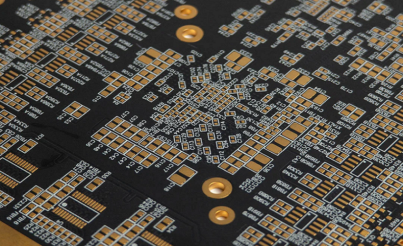
HDI PCB for automotive electronics is a high-density interconnect technology used in advanced vehicle systems such as ADAS radar modules, EV battery management systems, infotainment platforms, camera systems, and domain controllers. It enables compact layout integration, high-speed signal transmission, and long-term reliability under extreme temperature, vibration, and electrical noise conditions.
Automotive HDI PCB design must comply with IPC-6012 Class 3 reliability requirements, IPC-2221 design rules, and automotive qualification systems such as IATF 16949 and AEC-Q100. These requirements ensure consistent performance under -40°C to 125°C thermal cycling and long lifecycle operation exceeding 10–15 years.
Why HDI is Critical for Automotive Electronics
Automotive electronics are rapidly evolving into high-performance computing systems on wheels. HDI PCB technology is essential due to increased system integration and high-speed data requirements.
Key engineering drivers:
- ADAS radar systems require >10 Gbps signal channels
- EV battery management systems require dense sensor networks
- High-resolution cameras require controlled impedance routing
- ECU consolidation demands extreme miniaturization
Technical benefits:
- 40–70% reduction in PCB footprint
- Routing density >200 interconnects/cm²
- Reduced parasitic inductance in high-speed channels
- Improved EMI performance in automotive RF environments
Comparison:
- Standard PCB: low routing density, limited high-speed capability
- HDI PCB: high-density routing, controlled impedance, advanced integration
Miniaturization in Automotive Systems
Miniaturization is driven by ECU consolidation and electric vehicle platform integration.
HDI enables:
- Laser microvias replacing mechanical through vias
- Via-in-pad structures for fine-pitch BGA breakout
- Sequential lamination for vertical interconnect expansion
- Redistribution layers for IC-level routing density
Typical manufacturing values:
- BGA pitch: 0.4 mm–0.8 mm
- Microvia diameter: 0.075 mm–0.10 mm
- Trace width: 2.5–4.0 mil
- HDI layer structures: 1+N+1, 2+N+2 commonly used
Space optimization impact:
- ECU size reduction up to 60%
- Interconnect length reduction 30–50%
Signal Integrity in Automotive HDI PCB
Signal integrity is a critical factor in automotive high-speed systems such as radar, Ethernet, and imaging modules.
Electrical targets:
- Single-ended impedance: 50 ohm ±7%
- Differential impedance: 90–100 ohm
- Dielectric constant range: 3.2–4.5
- Loss tangent: <0.01 for high-speed channels
Engineering control methods:
- Continuous reference ground plane design
- Controlled impedance routing with tight tolerance
- Back-drilling to remove via stubs (>0.15 mm reduction)
- Differential pair matching tolerance ≤5 mil
Failure consequences:
- Radar signal distortion
- Camera frame jitter
- ECU communication delay and packet loss
Space Optimization in Automotive HDI PCB
Space optimization is a core requirement for modern automotive ECU architecture.
HDI solutions:
- 2+N+2 sequential lamination structures
- Microvia stacking for vertical routing
- Via-in-pad technology under fine-pitch BGAs
- High-density redistribution routing layers
Density improvements:
- Routing density increase up to 3×
- Layer utilization efficiency improved 30–40%
Automotive Manufacturing Standards
Automotive HDI PCB manufacturing requires strict compliance with global standards.
Key standards:
- IPC-6012 Class 3 (high reliability electronics)
- IPC-2221 (design spacing and electrical rules)
- IATF 16949 (automotive quality management system)
- AEC-Q100 (IC qualification standard)
Manufacturing tolerances:
- Layer registration: ±50 μm
- Microvia alignment: ±25 μm
- Impedance tolerance: ±7%
- Copper thickness variation: ±10%
Quality Certifications in Automotive HDI PCB
Automotive PCB suppliers must maintain strong process control systems.
Typical certifications:
- IATF 16949 automotive certification
- ISO 9001 quality system
- ISO 14001 environmental compliance
- IPC-A-600 acceptability standard
Quality inspection steps:
- Incoming material verification
- Laser drilling accuracy control
- X-ray via void inspection (<5% void requirement)
- TDR impedance validation
- Thermal stress qualification
Reliability Testing for Automotive HDI PCB
Automotive environments require extreme reliability validation.
Testing conditions:
- Thermal cycling: -40°C to 125°C, >1000 cycles
- Vibration testing: 10–2000 Hz random vibration
- Mechanical shock: 50G–150G impact
- Humidity resistance: 85°C / 85% RH for 1000 hours
Common failure mechanisms:
- Microvia cracking due to CTE mismatch
- Copper fatigue in vibration environments
- Delamination under thermal stress
Design Considerations in Automotive HDI PCB
Automotive HDI design must balance electrical, thermal, and mechanical constraints.
Key rules:
- Maintain symmetric stack-up to reduce warpage
- Ensure continuous ground return paths
- Avoid routing across split reference planes
- Maintain copper balance <10% difference
- Optimize via structure for minimal inductance
Line Width and Spacing Control
Line width and spacing directly affect impedance and signal integrity.
Manufacturing capability:
- Standard HDI: 3/3 mil
- Automotive HDI advanced: 2.5/2.5 mil
- Ultra HDI: 2/2 mil (low yield region)
Electrical sensitivity:
- 1 mil width variation ≈ 3–5 ohm impedance shift
- Spacing variation increases crosstalk up to 30%
Design rules:
- Single-ended spacing ≥3× trace width
- Differential pair spacing 5–7 mil typical
Thermal Management in Automotive HDI PCB
Thermal management is critical in EV and power systems.
Engineering methods:
- High Tg materials (>170°C)
- Thermal via arrays under power ICs
- Increased copper thickness in power layers
- Hybrid metal-core structures for high-power modules
Operating limits:
- Temperature range: -40°C to 125°C
- Junction temperature control: <150°C
Fabricator Evaluation for Automotive HDI PCB
Fabricator capability directly impacts reliability and yield.
Evaluation criteria:
- 0.075 mm microvia capability
- 20+ layer HDI stack-up support
- ±7% impedance control capability
- IATF 16949 compliance
- Proven automotive production history
Comparison:
- Basic fabricator: ±10–15% impedance control, limited HDI capability
- Automotive-grade fabricator: ±5–7% impedance, advanced sequential lamination
Real Factory Case Study
A 14-layer ADAS automotive HDI PCB was manufactured using 2+N+2 structure.
Initial issues:
- Impedance deviation: 58 ohm vs 50 ohm target
- Radar signal delay
- High-frequency jitter in differential channels
Root causes:
- Dielectric thickness variation ±12 μm
- Via stub length 0.20 mm
- Ground plane discontinuity near BGA region
Engineering corrections:
- Stack-up symmetry optimization
- Back-drilling to eliminate via stubs
- Trace width adjustment (-6%)
- Improved reference plane continuity
Final results:
- Impedance stabilized at 49–51 ohm
- Signal jitter reduced 28%
- Manufacturing yield improved from 87% to 95%
Common Design Errors
Frequent engineering mistakes:
- Late stack-up definition after routing
- Ignoring thermal expansion mismatch
- Overuse of microvias without reliability validation
- Routing over split ground planes
- Incorrect differential pair matching
FAQ
Why is HDI PCB important in automotive electronics?
Because it enables high-density integration, signal integrity, and miniaturization required for ADAS and EV systems.
What microvia size is used in automotive HDI PCB?
Typical laser microvia size is 0.075 mm–0.10 mm.
Which standards are required for automotive HDI PCB?
IPC-6012 Class 3, IPC-2221, and IATF 16949 are standard requirements.
What is the biggest reliability risk?
Thermal cycling-induced microvia cracking and CTE mismatch failures.


![Understanding PCB Costs & Pricing [Your Complete Guide]](https://hdicircuitboard.com/wp-content/uploads/elementor/thumbs/Understanding-PCB-Costs-Pricing-Your-Complete-Guide-qzzhe6mcaxuolkux3xalfktgavumi9y1aqfbs9bpv4.webp "Understanding PCB Costs & Pricing [Your Complete Guide]")


