







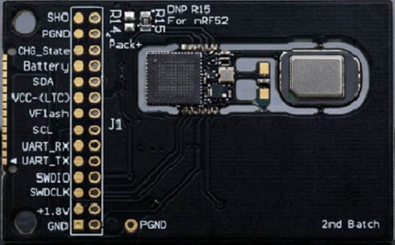
High density interconnect technology has become the preferred PCB architecture for modern IoT products because it combines miniaturization, electrical reliability, and manufacturing efficiency in a single platform. Compared with conventional multilayer boards, an hdi pcb supports finer routing, shorter signal paths, lower parasitic inductance, and improved power distribution while reducing overall board dimensions. For wearable electronics, smart sensors, industrial IoT gateways, healthcare monitors, and wireless communication modules, hdi circuit boards allow engineers to integrate more functions into smaller spaces without sacrificing reliability. Modern hdi pcb fabrication combines laser-drilled microvias, sequential lamination, via-in-pad plated over (VIPPO), precision impedance control, and advanced inspection methods to meet increasingly demanding electronic designs.
Why HDI Fits IoT & Wearables
Higher Functional Density
IoT devices continue becoming smaller while integrating more wireless interfaces, sensors, batteries, processors, and memory devices. Conventional multilayer boards often become routing limited before the mechanical enclosure reaches its final size.
An hdi pcb solves this problem by increasing routing density through:
- Laser microvias
- Blind vias
- Buried vias
- Fine line copper routing
- Via-in-pad plated over (VIPPO)
Typical production capability for an advanced hdi pcb manufacturer includes:
| Feature | Typical Production Capability |
|---|---|
| Line Width | 50–65 μm |
| Line Spacing | 50–65 μm |
| Laser Microvia | 75–100 μm |
| Finished Mechanical Via | 150–200 μm |
| Copper Thickness | 12–35 μm |
| Controlled Impedance | ±5% |
These capabilities allow designers to reduce PCB area by approximately 25–45% compared with traditional multilayer layouts.
Improved Assembly Efficiency
Reducing PCB size also reduces enclosure volume, assembly weight, connector length, and overall product complexity.
Typical wearable applications include:
- Smart watches
- Medical monitoring devices
- Smart glasses
- Wireless earbuds
- Fitness trackers
- Portable diagnostic equipment
Most products require battery-powered operation where every cubic millimeter matters.
Small Size
Compact Layout Strategy
Miniaturization begins during PCB stack-up planning.
Typical HDI stackups include:
- 1+N+1
- 2+N+2
- 3+N+3
Sequential lamination allows routing channels to be distributed layer by layer instead of depending entirely on through-hole vias.
For example, a six-layer IoT communication board may use:
- Layer 1: RF routing
- Layer 2: Ground
- Layer 3: Signal
- Layer 4: Power
- Layer 5: Signal
- Layer 6: Component placement
Using blind vias instead of through holes increases available routing channels by nearly 20%.
Mechanical Advantages
Smaller PCBs provide:
- Lower product weight
- Better vibration resistance
- Reduced connector stress
- Improved packaging flexibility
Typical wearable PCB thickness ranges from 0.4 mm to 0.8 mm.
Medical wearable products frequently specify finished board thickness below 0.6 mm.
Flexibility
Flexible Circuit Integration
Many wearable products cannot use rigid boards alone.
HDI Flex PCB combines:
- Polyimide flexible substrate
- HDI routing
- Laser microvias
- Dynamic bending capability
Common flex thickness:
- 25 μm
- 50 μm
- 75 μm polyimide
Copper thickness typically ranges from 12 μm to 18 μm.
Repeated dynamic bending often exceeds 100,000 cycles.
HDI Rigid Flex PCB
HDI Rigid Flex PCB combines rigid processing with flexible interconnections.
Advantages include:
- Elimination of board-to-board connectors
- Improved signal reliability
- Reduced assembly steps
- Better shock resistance
- Lower overall weight
Rigid-flex designs are increasingly adopted for healthcare wearables because connector failures are significantly reduced during long-term movement.
Better Signal
Signal Integrity
As wireless communication speeds increase, PCB routing becomes increasingly sensitive.
Typical IoT interfaces include:
- Wi-Fi
- Bluetooth
- BLE
- Zigbee
- Thread
- LTE
- GNSS
HDI routing improves signal quality by:
- Shorter trace length
- Smaller loop area
- Lower via inductance
- Reduced impedance discontinuity
Production targets commonly include:
- Differential impedance: 100 ±5 Ω
- Single-ended impedance: 50 ±5 Ω
EMI Reduction
Ground reference continuity becomes more important than additional copper.
Good HDI layout includes:
- Continuous reference planes
- Via stitching
- Ground return optimization
- Controlled transition vias
This reduces electromagnetic radiation while improving receiver sensitivity.
Design Terms
Sequential Lamination
Sequential lamination builds HDI layers one stage at a time.
Advantages:
- Higher routing density
- Better via reliability
- Improved layer registration
Typical lamination accuracy:
±50 μm
Via-in-Pad Plated Over
VIPPO allows BGA escape routing beneath component pads.
Benefits include:
- Reduced routing distance
- Better thermal performance
- Smaller package footprint
Copper-filled VIPPO structures are widely used for processors with pitch below 0.5 mm.
Microvias
Laser-drilled microvias are the foundation of modern hdi pcb fabrication.
Typical specifications:
| Parameter | Typical Value |
|---|---|
| Laser Drill Diameter | 75–100 μm |
| Maximum Aspect Ratio | ≤0.8:1 |
| Copper Filling | 100% Copper Filled |
| Thermal Cycling Reliability | >1000 Cycles |
Copper-filled microvias significantly reduce current crowding compared with partially plated vias.
Blind Vias
Blind vias connect outer layers to inner layers without penetrating the entire board.
Advantages include:
- Increased routing area
- Better impedance control
- Reduced stub length
- Lower parasitic capacitance
Typical blind via depth:
75–150 μm.
Buried Vias
Buried vias connect only internal layers.
They are used when:
- Routing density becomes extremely high.
- Outer layers require uninterrupted RF routing.
- Additional fan-out channels are necessary.
Combining buried vias with blind vias often increases routing efficiency by more than 30%.
What to Keep in Mind
Cost
HDI manufacturing increases fabrication cost because of:
- Laser drilling
- Sequential lamination
- Additional AOI inspection
- Copper filling
- Registration control
However, the finished product often reduces total system cost by decreasing enclosure size, connector quantity, cable length, and assembly complexity.
Power Use
Battery-powered devices require efficient power delivery.
Recommended design practices include:
- Wide power traces
- Low impedance return paths
- Multiple ground vias beneath processors
- Short battery connections
- Decoupling capacitors within 2–3 mm of power pins
Voltage drop should generally remain below 2% across major power rails.
HDI Flex PCB and HDI Rigid Flex PCB for the IoT
Selection Comparison
| Technology | Advantages | Typical Applications |
|---|---|---|
| Standard Multilayer PCB | Lower manufacturing cost, simple fabrication | Consumer electronics, industrial control |
| HDI PCB | Higher routing density, better signal integrity, smaller board size | IoT devices, communication modules, medical electronics |
| HDI Flex PCB | Dynamic bending capability with high-density routing | Wearables, smart sensors, foldable electronics |
| HDI Rigid-Flex PCB | Connector reduction, excellent mechanical reliability | Medical devices, aerospace, premium wearable products |
Selection depends on:
- Mechanical movement
- Product thickness
- Assembly volume
- Long-term reliability
Core Technical Parameters
Typical manufacturing capability of an experienced hdi pcb manufacturer:
- 3/3 mil (75/75 μm) production
- Advanced 2/2 mil capability for selected designs
- Laser microvia: 75 μm
- Finished via: 0.15 mm
- Sequential lamination: up to 3+N+3
- Copper-filled VIPPO
- Resin plug technology
- ENIG surface finish
- Impedance tolerance: ±5%
- CAF prevention material selection
- Tg170–180 high reliability laminates
- Low-loss materials for RF applications
Factory Case Study
A customer developing a medical wearable ECG recorder required a six-layer HDI design measuring only 32 × 28 mm.
Original design:
- Six layers
- 1+N+1 stackup
- 0.6 mm thickness
- 0.4 mm BGA
- 3/3 mil routing
- Laser microvias
Initial production issues:
- BGA solder voids
- Microvia misregistration
- Impedance variation beyond specification
Engineering improvements:
- Increased laser alignment verification frequency
- Optimized copper filling parameters
- Modified lamination pressure profile
- Added X-ray inspection before assembly
- Controlled dielectric thickness within ±15 μm
Final results:
- Yield improved from 91.4% to 98.3%
- Impedance remained within ±4%
- Assembly defect rate reduced by 43%
- Signal eye diagram passed customer validation
Common Design Errors
Typical production issues observed by factory engineers include:
- Using through-hole vias beneath fine-pitch BGAs
- Excessive microvia stacking without reliability verification
- Ignoring return current paths
- Mixing RF and switching power routing
- Copper imbalance causing board warpage
- Overly aggressive trace width beyond fabrication capability
- Incorrect solder mask clearance around VIPPO
- Insufficient teardrop design near laser vias
These problems often increase manufacturing cost more than material selection itself.
Quality Control
Reliable hdi pcb fabrication includes:
- Incoming laminate inspection
- Laser drill calibration
- AOI after every imaging stage
- Cross-section verification
- Copper thickness measurement
- Flying probe electrical testing
- X-ray inspection
- Thermal shock testing
- IST reliability testing
- Peel strength verification
- Final impedance testing
Design guidance follows IPC-2221, while qualification and workmanship requirements align with IPC-6012 where applicable.
FAQ
What makes HDI PCB better than conventional multilayer PCB?
HDI routing increases circuit density, reduces signal path length, improves electrical performance, and enables significantly smaller electronic products.
When should designers choose blind vias instead of through vias?
Blind vias are preferred whenever routing space beneath BGAs or RF components becomes limited and signal stubs need to be minimized.
Is HDI Flex PCB more reliable than standard flex PCB?
For wearable products requiring dense routing, HDI Flex PCB provides better electrical performance while maintaining excellent bending capability when proper bend radius rules are followed.
How many sequential laminations are practical for mass production?
Most commercial designs use 1+N+1 or 2+N+2 structures. Advanced communication products may adopt 3+N+3 when routing density justifies the additional manufacturing complexity.

![Understanding PCB Costs & Pricing [Your Complete Guide]](https://hdicircuitboard.com/wp-content/uploads/elementor/thumbs/Understanding-PCB-Costs-Pricing-Your-Complete-Guide-qzzhe6mcaxuolkux3xalfktgavumi9y1aqfbs9bpv4.webp "Understanding PCB Costs & Pricing [Your Complete Guide]")