







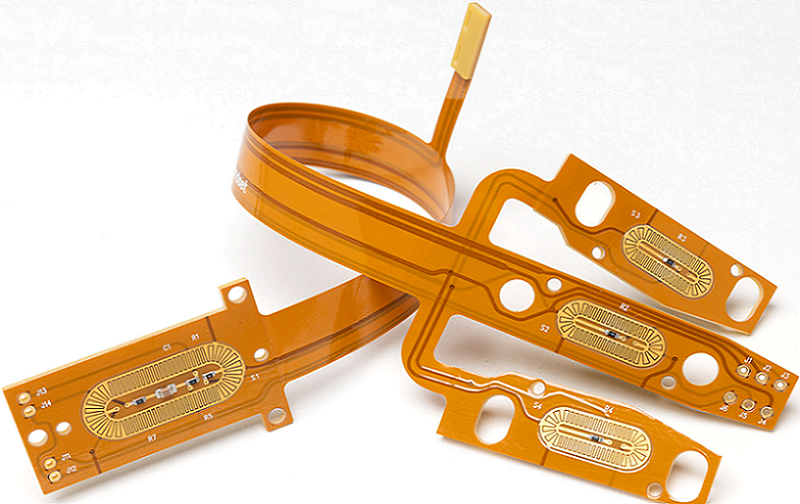
Flexible PCB manufacturing services provide advanced circuit solutions for electronic products that require lightweight structures, compact packaging, and mechanical flexibility. Unlike rigid PCB solutions based on FR-4 laminates, flexible circuits use polyimide-based materials and specialized copper structures to support bending, folding, and three-dimensional installation. A professional flexible PCB manufacturer must control material selection, fine-line fabrication, copper reliability, impedance performance, and assembly processes to deliver stable products for medical, automotive, semiconductor, aerospace, and industrial applications.
A reliable flexible PCB supplier should provide complete support from flexible PCB Prototype development to mass production, including DFM analysis, material recommendation, stack-up design, fabrication process control, electrical testing, and assembly services. Advanced flexible PCB fabrication requires compliance with industry standards such as IPC-2223 and IPC-6013 while maintaining precise control of copper thickness, trace geometry, bend radius, and reliability performance.
Flexible PCB Manufacturing Capabilities
Advanced Flexible Circuit Structures
Flexible PCB manufacturing requires specialized processes because flexible materials behave differently from traditional rigid laminates. The circuit must maintain electrical performance while experiencing mechanical deformation.
Common flexible PCB structures include:
- Single-layer flexible PCB
- Double-layer flexible PCB
- Multi-layer flexible PCB
- Rigid-flex PCB
- High-density flexible PCB with microvias
Typical manufacturing capability ranges include:
| Capability Item | Typical Range |
|---|---|
| Flexible PCB Layers | 1–12 layers |
| Advanced Rigid-Flex Layers | 20+ layers |
| Board Thickness | 0.05–0.30 mm |
| Copper Thickness | 12 μm–70 μm |
| Minimum Line Width/Spacing | 50 μm / 50 μm (2/2 mil) |
| Standard Line Width/Spacing | 75 μm / 75 μm (3/3 mil) |
| Microvia Diameter | 0.075–0.15 mm |
| Controlled Impedance Tolerance | ±7% to ±10% |
For semiconductor equipment and high-speed applications, flexible PCB manufacturing must also consider signal integrity, dielectric thickness variation, and impedance stability.
Flexible PCB Fabrication Process Control
A complete flexible PCB fabrication process includes:
- Material preparation
- Inner layer circuit imaging
- Copper etching
- Layer lamination
- Laser drilling
- Copper plating
- Coverlay lamination
- Surface finishing
- Electrical testing
- Final inspection
Compared with rigid PCB production, flexible PCB fabrication requires tighter control of:
- Material expansion coefficient
- Lamination pressure
- Coverlay alignment
- Copper stress distribution
- Mechanical bending performance
Flexible PCB Materials
Base Materials for Flexible Circuits
Material selection determines the electrical, thermal, and mechanical performance of flexible PCB products.
The most common base materials include:
| Material | Main Characteristics | Typical Application |
|---|---|---|
| Polyimide (PI) | High temperature resistance, excellent flexibility | Medical, automotive, industrial electronics |
| Liquid Crystal Polymer (LCP) | Low dielectric loss, low moisture absorption | RF and high-speed circuits |
| Adhesiveless PI | Better dimensional stability and reliability | High-reliability flexible circuits |
Polyimide is the most widely used material in flexible PCB manufacturing because it provides:
- Operating temperature range:
- Approximately -55°C to +125°C
- Excellent chemical resistance
- High dimensional stability
- Good mechanical durability
Copper Material Selection
Copper selection is critical for flexible PCB reliability.
Common copper types:
| Copper Type | Characteristics | Application |
|---|---|---|
| Rolled Annealed Copper (RA Copper) | High flexibility and excellent fatigue resistance | Dynamic bending applications |
| Electro Deposited Copper (ED Copper) | Good electrical performance and standard reliability | Static flexible PCB applications |
RA copper is preferred for repeated bending applications because its grain structure provides better fatigue resistance.
Typical copper thickness:
- 12 μm
- 18 μm
- 35 μm
- 70 μm
For dynamic bending circuits, thinner RA copper such as 12–18 μm is commonly selected to reduce mechanical stress.
Manufacturing Techniques for Flexible PCB Fabrication
Circuit Formation and Layer Processing
Flexible PCB fabrication uses precision manufacturing techniques to create reliable copper patterns on thin dielectric films.
Important processes include:
- Photolithography
- Precision etching
- Laser drilling
- Electroplating
- Coverlay processing
- Surface finishing
For advanced flexible PCB Prototype projects, manufacturers often perform additional engineering validation:
- Material evaluation
- Stack-up optimization
- Mechanical simulation
- Electrical verification
Copper Traces and Reliability Control
Copper traces are one of the most critical reliability factors in flexible PCB manufacturing.
Poor trace design may cause:
- Copper fatigue cracking
- Open circuits
- Signal instability
Recommended trace design practices:
- Use curved routing instead of sharp corners
- Avoid 90-degree trace angles
- Maintain consistent copper width
- Avoid vias inside bending areas
Typical trace requirements:
| Parameter | Recommended Value |
|---|---|
| Minimum Trace Width | 50–75 μm |
| Minimum Trace Spacing | 50–75 μm |
| Dynamic Bend Copper Thickness | 12–18 μm |
| Static Bend Copper Thickness | 18–35 μm |
Flexible PCB Assembly Services
SMT Assembly for Flexible Circuits
Flexible PCB assembly requires additional process controls compared with rigid PCB assembly.
Key manufacturing requirements include:
- Temporary carrier support
- Controlled solder paste printing
- Accurate component placement
- Optimized reflow profile
Typical SMT parameters:
| Process Parameter | Typical Value |
|---|---|
| Component Placement Accuracy | ±25 μm |
| Reflow Temperature | 230–250°C |
| Fine Pitch Capability | 0.3–0.5 mm |
Flexible PCB assembly requires careful thermal management because thin materials transfer heat differently compared with rigid boards.
Rigid-Flex PCB Assembly
Rigid-flex assembly combines rigid PCB sections with flexible circuit areas.
Advantages:
- Reduced connectors
- Lower assembly complexity
- Improved reliability
- Smaller product size
Common applications:
- Aerospace systems
- Medical equipment
- Semiconductor test systems
Flexible PCB Design and Manufacturing Guidelines
Bend Radius Requirements
Bend radius is one of the most important design parameters in flexible PCB manufacturing.
The correct bend radius prevents:
- Copper cracking
- Dielectric damage
- Layer separation
Typical guidelines:
| Application | Bend Radius |
|---|---|
| Static Bend | 5–10× Total Thickness |
| Dynamic Bend | Greater than 10× Thickness |
| Repeated Bending Application | Requires Mechanical Reliability Testing |
For dynamic applications, engineers usually select:
- RA copper
- Thin dielectric layers
- Balanced stack-up design
A flexible PCB Prototype intended for repeated movement should be tested under actual mechanical conditions.
Trace Routing Guidelines
Flexible PCB routing must consider mechanical stress.
Recommended practices:
- Place traces along the bending direction
- Avoid abrupt width changes
- Avoid copper concentration imbalance
- Keep components away from bending zones
Incorrect routing may create stress concentration areas that reduce product lifetime.
Flexible PCB Quality Standards
Industry Standards
Professional flexible PCB suppliers follow international PCB standards:
- IPC-2223: Flexible Printed Board Design Standard
- IPC-6013: Flexible Printed Board Qualification and Performance Specification
- IPC-A-600: Printed Board Acceptability
- IPC-A-610: Electronic Assembly Acceptability
Quality Control Process
Typical quality inspection includes:
- AOI inspection
- Electrical continuity testing
- Insulation resistance testing
- Microsection analysis
- Copper thickness measurement
- Coverlay inspection
- Impedance testing
Critical quality parameters include:
- Layer registration
- Copper adhesion
- Via reliability
- Dimensional stability
- Bend cycle performance
Flexible PCB Manufacturing Case Study
4-Layer Flexible PCB for Semiconductor Equipment
A semiconductor equipment customer required a high-reliability flexible circuit with repeated mechanical movement.
Product structure:
- 4-layer flexible PCB
- Polyimide base material
- 18 μm RA copper
- 0.15 mm finished thickness
- 75 μm line width and spacing
- Controlled impedance requirement: ±7%
Manufacturing Challenge
Initial evaluation identified:
- Copper stress concentration near bending area
- Coverlay alignment variation
- Impedance fluctuation caused by thickness variation
Engineering Improvement
The manufacturing team optimized:
- Trace routing with curved patterns
- RA copper selection
- Coverlay registration tolerance
- Lamination parameters
Results:
- Improved bending reliability
- Reduced copper cracking risk
- Improved electrical consistency
- Increased production yield
Common Flexible PCB Design Errors
Incorrect Bend Area Design
Placing components or vias inside bending zones can create mechanical failure.
Common problems:
- Copper cracking
- Layer separation
- Reduced bending cycles
Incorrect Material Selection
Selecting inappropriate materials may affect:
- Thermal performance
- Signal integrity
- Mechanical reliability
Excessive Trace Density
Overly aggressive routing can create:
- Manufacturing difficulty
- Higher defect rates
- Reduced reliability
Leading Flexible PCB Service Providers
San Francisco Circuits
Provides flexible and rigid flex PCB solutions supporting prototype and production requirements.
Sierra Circuits
Offers flexible PCB fabrication services with engineering support and advanced PCB manufacturing capability.
TTM Technologies
Provides flexible and rigid-flex PCB manufacturing solutions for automotive, aerospace, medical, and industrial markets.
Benchuang Electronics
Benchuang Electronics provides high-reliability PCB manufacturing capability including:
- Flexible PCB
- Rigid-Flex PCB
- Advanced HDI PCB
- High-layer-count PCB
The company supports complex PCB requirements through:
- Advanced manufacturing processes
- Controlled impedance capability
- Engineering collaboration
- High-mix low-volume production
FAQ
Q1: What is flexible PCB manufacturing?
Answer:
Flexible PCB manufacturing is the process of producing flexible electronic circuits using materials such as polyimide and RA copper. It enables lightweight, compact, and bendable electronic designs.
Q2: What materials are used in flexible PCB fabrication?
Answer:
The most common materials are polyimide, LCP, adhesiveless flexible laminates, and rolled annealed copper. Material selection depends on electrical, thermal, and mechanical requirements.
Q3: What is the minimum bend radius of a flexible PCB?
Answer:
The minimum bend radius depends on thickness, copper type, and bending frequency. Static applications typically require 5–10 times thickness, while dynamic applications require larger radius and reliability validation.
Q4: How do I select a flexible PCB manufacturer?
Answer:
Engineers should evaluate manufacturing capability, material control, quality standards, prototype support, assembly capability, and engineering experience before selecting a flexible PCB supplier.

![Understanding PCB Costs & Pricing [Your Complete Guide]](https://hdicircuitboard.com/wp-content/uploads/elementor/thumbs/Understanding-PCB-Costs-Pricing-Your-Complete-Guide-qzzhe6mcaxuolkux3xalfktgavumi9y1aqfbs9bpv4.webp "Understanding PCB Costs & Pricing [Your Complete Guide]")