







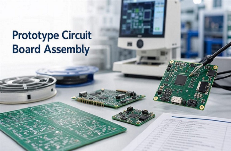
A reliable pcb prototype and assembly project is not simply a fast version of production PCB manufacturing. It is a controlled engineering loop that converts design files into a fabricated board, sources the correct PCB components, assembles the prototype printed circuit, and verifies electrical and mechanical performance before production release. A practical prototype PCB flow is design files → DFM review → pcb board fabrication → component sourcing → prototype PCB assembly → inspection → electrical testing → engineering revision. For a typical 4-layer FR-4 prototype, representative starting parameters are 1.6 mm finished thickness, 1 oz copper, 5/5 mil minimum line/space, 0.20–0.30 mm finished vias, and 50 Ω controlled impedance where required. These values are engineering examples rather than universal limits; the final values must follow the selected fabricator, material stack-up, component package, and IPC requirements.
PCB Prototyping Process
Design Files and Engineering Data
The first stage of pcb prototyping is converting the electrical design into manufacturing data. A prototype PCB fabrication package should contain enough information for both board manufacturing and assembly.
Core files normally include:
- Gerber or ODB++ copper and mask data
- NC drill files
- PCB fabrication drawing
- Stack-up information
- Bill of materials
- Pick-and-place centroid file
- Assembly drawings
- Component datasheets
- Special process requirements
- Controlled-impedance requirements where applicable
For a standard 4-layer prototype, a fabrication drawing may define:
| Parameter | Example Production Value |
|---|---|
| Layers | 4 |
| Finished thickness | 1.60 ±0.16 mm |
| Outer copper | 1 oz |
| Inner copper | 1 oz |
| Minimum line/space | 5/5 mil |
| Finished mechanical via | 0.25 mm |
| Minimum annular ring | 0.10 mm |
| Solder mask dam | 4–5 mil |
| Controlled impedance | 50 Ω / 100 Ω |
| Surface finish | ENIG |
The engineering value of this stage is traceability. If the prototype fails, the team needs to determine whether the problem originated in the schematic, PCB layout, fabrication, component, or assembly process.
DFM and Stack-Up Review
A printed circuit board prototype should undergo a manufacturing review before fabrication.
The review should examine:
- Minimum copper width
- Minimum spacing
- Drill-to-copper clearance
- Annular ring
- Copper-to-edge clearance
- Solder-mask openings
- BGA escape geometry
- Via-in-pad requirements
- Controlled impedance
- Copper balance
- Layer symmetry
- Board thickness
For HDI PCB prototypes, additional parameters can include:
- 6-layer or 8-layer construction
- 1+N+1 or 2+N+2 HDI structure
- 0.10–0.15 mm laser microvias
- 0.20–0.30 mm capture pads
- 3/3–4/4 mil line/space
- 50 Ω single-ended routing
- 85–100 Ω differential routing
The principle is straightforward: the CAD design defines the intended circuit, while DFM determines whether the intended geometry can actually be fabricated repeatedly.
PCB Board Fabrication
Material Selection and Layer Construction
The substrate affects electrical, mechanical, thermal, and manufacturing performance.
Common prototype materials include:
- Standard FR-4
- High-Tg FR-4
- Low-loss laminate
- Polyimide for flex circuits
- Metal-core materials for thermal applications
A standard 4-layer FR-4 prototype may use a stack-up such as:
- L1 signal
- L2 ground
- L3 power
- L4 signal
Keeping high-speed signal layers adjacent to continuous reference planes reduces return-current discontinuity and helps maintain controlled impedance.
For a high-speed prototype printed circuit, the dielectric thickness between signal and reference plane may be around 3–8 mil depending on the required impedance and laminate system.
Fabrication Process
The pcb manufacturing sequence normally includes:
- Material cutting
- Inner-layer imaging
- Etching
- AOI
- Lamination
- Drilling
- Desmear
- Through-hole plating
- Outer-layer imaging
- Copper plating
- Etching
- Solder-mask application
- Surface finishing
- Legend printing
- Routing
- Electrical testing
A prototype PCB may use ENIG with approximately 3–6 µin gold over nickel thickness around 100–200 µin, depending on the specified finish and supplier process.
For HASL, the surface is coated with solder alloy rather than electroless nickel/gold. ENIG generally provides a flatter surface for fine-pitch SMT components and BGA packages.
Component Sourcing
BOM Verification
Component sourcing is often underestimated during circuit board prototyping.
The BOM should be checked for:
- Manufacturer part number
- Package type
- Quantity
- Lifecycle status
- Approved alternatives
- Voltage rating
- Current rating
- Tolerance
- Temperature rating
- Moisture sensitivity level
- Lead time
A PCB prototype cannot validate the design if the assembly uses an electrically different substitute.
For example, two 10 kΩ resistors may have identical resistance but different:
- Tolerance
- Power rating
- Package
- Temperature coefficient
- Voltage coefficient
- Manufacturer specifications
Component Quality Control
Incoming components should be controlled using:
- Manufacturer labels
- Lot identification
- Date codes
- Certificate of conformance where required
- Moisture-sensitive-device handling
- Counterfeit screening for critical components
For fine-pitch prototypes, package verification is particularly important. A 0.4 mm-pitch BGA has far less assembly tolerance than a 2.54 mm-pitch through-hole connector.
Prototype PCB Assembly
SMT Assembly
A typical prototype PCB assembly starts with solder-paste printing.
The process includes:
- Apply a stainless-steel stencil.
- Align stencil apertures with PCB pads.
- Print solder paste using a controlled squeegee process.
- Inspect paste deposition.
- Pick and place components.
- Reflow solder the assembly.
- Perform post-reflow inspection.
A practical stencil may be:
- 0.10–0.15 mm thick for fine-pitch SMT
- 0.15–0.20 mm for general SMT
- Locally reduced around small-pitch components
For a 0.5 mm-pitch QFP, excessive paste volume can create bridging. For a large thermal pad, insufficient paste can produce voiding or inadequate thermal transfer.
THT and Mixed Assembly
Through-hole assembly remains important for:
- Large connectors
- Transformers
- Relays
- High-mechanical-load components
- Power components
A mixed-technology prototype can combine SMT and THT in the same assembly.
Typical sequence:
- SMT paste printing
- SMT placement
- Reflow
- THT insertion
- Selective soldering or hand soldering
- Inspection
- Electrical testing
The correct process depends on component geometry and mechanical requirements rather than simply minimizing assembly steps.
Prototype PCB Assembly Options
Turnkey Assembly
A turnkey provider handles:
- PCB fabrication
- Component procurement
- PCB assembly
- Inspection
- Testing
- Final shipment
This approach reduces the number of interfaces between engineering and manufacturing.
It is particularly effective when the prototype requires:
- PCB fabrication
- 20–200 assembled boards
- 100+ unique components
- SMT and THT
- Multiple component suppliers
- Full traceability
The engineering advantage is centralized responsibility.
Consigned / Kitted Assembly
With consigned or kitted assembly, the customer supplies some or all components while the manufacturer performs the assembly.
This is useful when:
- Components are already in inventory
- Specific manufacturer parts are mandatory
- Proprietary components are involved
- Customer-controlled components must be used
The main manufacturing variable becomes material completeness.
A single missing 0.1 µF capacitor can stop an entire prototype build if the assembly line cannot substitute it.
In-House DIY
In-house assembly can be practical for very small quantities.
A basic laboratory setup may include:
- Stencil printer
- Hot plate or small reflow oven
- Pick-and-place equipment
- Microscope
- Multimeter
- Bench power supply
- Oscilloscope
It becomes less attractive when the prototype contains 0.4 mm BGAs, QFNs with exposed thermal pads, dense HDI routing, or more than 100 placements per board.
Two Key Prototype Comparisons
Turnkey vs Consigned / Kitted
| Factor | Turnkey | Consigned / Kitted |
|---|---|---|
| PCB fabrication | Manufacturer | Manufacturer |
| Component sourcing | Manufacturer | Customer |
| BOM responsibility | Shared through approved process | Primarily customer |
| Purchasing workload | Lower | Higher |
| Proprietary parts | Requires coordination | Easier |
| Supply-chain control | Manufacturer-controlled | Customer-controlled |
| Prototype speed | High when sourcing is available | High when kits are complete |
| Material shortage risk | Managed by sourcing team | Customer-managed |
Prototype vs Production PCB
| Factor | Prototype PCB | Production PCB |
|---|---|---|
| Quantity | 1–500 typical engineering range | Hundreds to millions |
| Primary objective | Validation | Repeatability and cost |
| Engineering changes | Frequent | Controlled |
| DFM flexibility | Higher | Lower |
| Test coverage | Engineering-focused | Production-focused |
| Fixture investment | Often minimized | Often justified |
| Component sourcing | Small-lot availability | Long-term supply |
| Process optimization | Fast iteration | Statistical control |
Testing and Quality Control
Inspection
A professional prototype PCB assembly should include inspection appropriate to board complexity.
Common inspection methods include:
- Automated Optical Inspection
- X-ray inspection
- Microscope inspection
- Solder-joint inspection
- Dimensional inspection
- Component presence verification
X-ray is particularly valuable for:
- BGA
- QFN
- Bottom-terminated components
- Hidden solder joints
- Via-in-pad structures
AOI is efficient for visible SMT joints but cannot directly see the center balls of a BGA.
Electrical Testing
Electrical testing should be defined before assembly.
Typical checks include:
- Continuity
- Isolation
- Resistance
- Power-rail verification
- Programming
- Functional test
- Communication-interface test
For example, a prototype controller may require:
- 5 V input verification
- 3.3 V rail verification
- 1.2 V core-rail verification
- USB communication
- Ethernet link
- ADC measurement
- MCU programming
The prototype should not be considered electrically validated simply because every solder joint looks acceptable.
Real Factory Prototype Case
8-Layer Computing Prototype
A practical engineering example involves an 8-layer computing board containing:
- 8-layer FR-4
- 1.60 mm finished thickness
- High-Tg laminate
- 1 oz outer copper
- 0.5 mm-pitch BGA
- 4/4 mil minimum routing
- 0.20 mm mechanical vias
- 100 Ω differential interfaces
- 50 Ω single-ended high-speed signals
- Approximately 420 SMT placements
The first pcb prototype and assembly build produced intermittent high-speed link failures.
Manufacturing Investigation
The assembly joints passed AOI, and electrical continuity passed.
The engineering review found:
- One differential pair had a 14 mm longer route than its companion.
- A high-speed transition passed through a reference-plane discontinuity.
- Several BGA escape traces used unnecessarily long via transitions.
- Decoupling capacitors were positioned 18–22 mm from selected power pins.
Corrective Action
The revised PCB design:
- Reduced differential-pair mismatch to below 5 mm.
- Restored continuous reference-plane routing.
- Reduced critical via transitions.
- Moved selected 100 nF capacitors within approximately 2–4 mm of processor power pins.
- Added impedance verification coupons.
The second prototype passed the intended high-speed functional test.
The manufacturing lesson is significant: prototype PCB assembly problems are not always soldering problems. A board can have 100% visually acceptable assembly while failing because of routing, return-path, impedance, power-distribution, or component-placement issues.
Common Production Design Errors
Incorrect Manufacturing Rules
Common examples include:
- 3 mil spacing on a standard low-cost process
- 0.10 mm finished holes without specifying laser drilling
- Insufficient annular ring
- Excessive copper density
- BGA escape geometry below fabrication capability
A prototype should use manufacturing rules tied to the actual fabricator.
Incomplete Assembly Data
Frequent assembly-release problems include:
- Missing polarity markings
- Incorrect pin 1 orientation
- Wrong centroid rotation
- Missing DNP information
- BOM manufacturer numbers inconsistent with footprints
- Incorrect paste-layer openings
These errors can survive PCB fabrication because the board itself may be physically correct.
Treating Substitutes as Identical
A replacement component should be checked for:
- Electrical equivalence
- Package compatibility
- Thermal performance
- Pin compatibility
- Availability
- Qualification requirements
Replacing an automotive-grade component with a commercial-grade part may make the prototype function while invalidating the intended product qualification path.
Prototype PCB Assembly Release Checklist
Before releasing a prototype printed circuit board, verify:
- Schematic revision is frozen
- PCB revision matches schematic
- BOM revision is controlled
- Manufacturer part numbers are verified
- Footprints match datasheets
- Gerber or ODB++ data is checked
- NC drill files are verified
- Stack-up is approved
- Minimum line/space is manufacturable
- Via dimensions are manufacturable
- Impedance requirements are defined
- Assembly drawing is complete
- Pick-and-place data is verified
- DNP components are identified
- Test requirements are documented
- Inspection criteria are defined
- Engineering revision is recorded
FAQ
What Is Prototype PCB Assembly?
Question: What does prototype PCB assembly include?
Answer: Prototype PCB assembly converts a fabricated bare PCB into a functional assembled board by applying solder paste, placing PCB components, reflowing or soldering the components, inspecting solder joints, and performing electrical or functional testing. A complete prototype PCB assembly project may also include PCB manufacturing, component sourcing, programming, conformal coating, and final packaging.
What Is the Difference Between Turnkey and Consigned Assembly?
Question: Should I use turnkey or consigned prototype PCB assembly?
Answer: Turnkey assembly places PCB fabrication and component procurement under the assembly supplier, while consigned or kitted assembly allows the customer to supply some or all components. Turnkey reduces purchasing workload; consigned assembly provides greater control over proprietary or customer-selected components.
What Files Are Required for PCB Prototyping?
Question: What files are needed to manufacture and assemble a PCB prototype?
Answer: A complete release normally includes Gerber or ODB++ fabrication data, NC drill files, fabrication drawings, stack-up information, BOM, pick-and-place data, assembly drawings, component specifications, and testing requirements. For controlled-impedance or HDI designs, impedance targets, material data, via structures, and relevant fabrication requirements should also be documented.
How Many PCB Prototypes Should Be Built?
Question: How many PCB prototypes are required before production?
Answer: There is no universal quantity. A simple 2-layer board may require only 3–10 units for electrical validation, while a complex 8–16-layer board with BGA, controlled impedance, power integrity, and multiple interfaces may require 20–100 units across engineering revisions. The appropriate quantity depends on design maturity, component risk, test coverage, and the number of manufacturing variables that must be validated.

![Understanding PCB Costs & Pricing [Your Complete Guide]](https://hdicircuitboard.com/wp-content/uploads/elementor/thumbs/Understanding-PCB-Costs-Pricing-Your-Complete-Guide-qzzhe6mcaxuolkux3xalfktgavumi9y1aqfbs9bpv4.webp "Understanding PCB Costs & Pricing [Your Complete Guide]")