







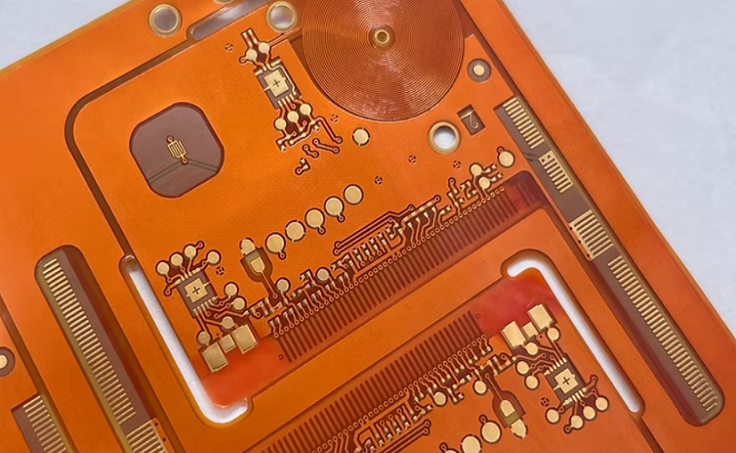
Flexible PCB design succeeds when the mechanical bend, copper pattern, dielectric stack-up, coverlay, stiffeners, and component zones are engineered as one system. For static installations, a practical bend radius often begins at 6–10 times the finished flex thickness; dynamic circuits may require 50–100 times thickness, rolled-annealed copper, and a symmetrical stack-up. Vias, pads, component lands, stiffener edges, and abrupt trace transitions must remain outside the bending zone. These rules allow a flexible PCB manufacturer to control copper strain, prevent coverlay separation, maintain impedance, and move a flexible PCB prototype into stable production. IPC-2223 defines specific design requirements for flexible and rigid-flex printed boards, while IPC-6013 covers their qualification and performance requirements.
Flexible PCB Design Scope
Define the Flex Function
Every flexible PCB design should begin by classifying the mechanical function:
- Flex-to-install: The circuit is bent during assembly and remains fixed.
- Service flex: The circuit moves occasionally during maintenance.
- Dynamic flex: The circuit bends repeatedly during normal operation.
- Rigid-flex: Flexible layers connect rigid component sections.
This classification controls the allowable layer count, copper type, finished thickness, and bend radius. A two-layer flex that bends once can use a substantially tighter geometry than a six-layer construction expected to complete one million cycles.
The fabrication drawing should state:
- Bend location and bend direction
- Final bend angle
- Required bend radius
- Expected number of cycles
- Flex-to-install or dynamic classification
- Component and stiffener boundaries
- Controlled impedance requirements
- Finished flex thickness
Without these inputs, a flexible PCB supplier can manufacture the artwork but cannot reliably validate its mechanical life.
Separate Electrical and Mechanical Zones
A practical layout divides the circuit into three zones:
- Dynamic flex zone
- Traces and dielectric only
- No plated holes
- No component pads
- No stiffener transitions
- Transition zone
- Gradual change from flexible to reinforced construction
- Curved trace fanout
- Controlled coverlay and adhesive overlap
- Rigid or reinforced zone
- Components
- Connectors
- Test pads
- Plated through holes
- Local stiffeners
This zoning prevents electrical features from being placed where repeated tensile and compressive strain is highest.
Bending and Layout Rules
Bend Radius by Construction
Bend radius is measured to the inside surface of the flex. The required value increases with total thickness, copper layers, adhesive thickness, and cycle count.
| Flex Construction | Static Bend Radius | Dynamic Bend Radius |
|---|---|---|
| Single-layer flex | 6–10× thickness | 50–100× thickness |
| Double-layer flex | 10–15× thickness | 75–100× thickness |
| Multilayer flex | 15–25× thickness | Application testing required |
| Four-layer bonded flex | 20–30× thickness | Normally avoided for continuous motion |
Industry guidance commonly uses approximately 6–10 times thickness for static bending, while multilayer or dynamic designs require much larger radii. Published fabrication guidance also places multilayer static bends near 15–20 times thickness or more.
For a 0.20 mm double-layer static flex:
- Minimum starting radius at 10× thickness: 2.0 mm
- More conservative radius at 15× thickness: 3.0 mm
For a 0.15 mm dynamic flex at 100× thickness:
- Target bend radius: 15 mm
These values are starting design limits rather than guaranteed cycle-life values. Final validation requires the actual stack-up, bend angle, travel distance, temperature, and operating frequency.
Keep the Bend Uniform
The bend area should have constant width and thickness. Local thickness changes shift the neutral axis and create concentrated strain.
The bend region should not contain:
- Copper pours with abrupt boundaries
- Plated through holes
- Laser vias
- Surface-mount pads
- Stiffener edges
- Coverlay termination steps
- Sudden changes in trace width
- Notches with sharp internal corners
For a 90-degree installed bend, the flexible section should extend beyond the bend tangent on both sides. A practical straight allowance of 1.0–2.0 mm outside each tangent prevents the bend from starting directly at a rigid interface.
Bend Radius Control
Copper Strain Mechanism
During bending, copper on the outside radius is stretched while copper on the inside radius is compressed. The neutral axis experiences the lowest strain.
Copper strain rises when:
- Finished thickness increases
- Bend radius decreases
- Copper is positioned far from the neutral axis
- Adhesive layers create an asymmetric stack-up
- Traces cross the bend at an angle
- Multiple copper layers overlap directly
A symmetrical two-layer stack-up places the copper layers at similar distances from the neutral axis. For dynamic flex, this symmetry improves fatigue life and reduces directional curl.
Static and Dynamic Comparison
| Design Factor | Static Flex | Dynamic Flex |
|---|---|---|
| Expected movement | One installation bend | Repeated operating cycles |
| Common copper | RA or ED copper | RA copper |
| Typical copper thickness | 18–35 µm | 12–18 µm |
| Typical bend radius | 6–15× thickness | 50–100× thickness |
| Vias in bend area | Not acceptable | Not acceptable |
| Trace pattern | Curved and uniform | Curved, uniform, and parallel |
| Qualification | Forming inspection | Cycle testing |
A flexible PCB prototype for a dynamic product should be tested in the actual bend direction. A coupon bent in the opposite direction does not reproduce the same copper strain.
Trace Routing Rules
Route Perpendicular to the Bend
Traces should cross the bend line at approximately 90 degrees. Routing diagonally through the bend creates uneven trace length across the bend and concentrates strain along one edge.
Inside a dynamic flex zone:
- Keep traces straight through the primary bend
- Use curved transitions before entering the bend
- Avoid 90-degree corners
- Use arc radii of at least 0.5 mm where space permits
- Maintain constant conductor width
- Keep adjacent trace spacing uniform
For production-oriented flexible PCB fabrication:
- Standard trace width and spacing: 75/75 µm
- Advanced capability: 50/50 µm
- Preferred dynamic trace width: 100 µm or greater
- Controlled impedance tolerance: typically ±10%
- Tighter controlled processes: ±7%
A 50 µm trace may be manufacturable, but it is mechanically less tolerant than a 100 µm trace in a repeated bend. Manufacturability and flex life are separate design limits.
Stagger Copper Between Layers
Directly overlapping traces in a double-layer flex increase local stiffness and concentrate stress. Staggering conductors between layers distributes copper more evenly and improves flexibility. Design guidance for dynamic double-sided circuits specifically discourages routing traces directly above each other in the same direction.
A practical offset is:
- Trace pitch: 0.25 mm
- Layer-to-layer trace offset: 0.125 mm
This creates a staggered pattern while maintaining a balanced copper distribution.
Cross-hatched shielding should use:
- Copper opening ratio: 40–60%
- Hatch angle: 45 degrees
- Minimum web width: 100–150 µm
Solid copper planes should remain outside dynamic bending areas unless electrical performance makes them unavoidable.
No Vias in Bending Zones
Via Exclusion Distance
Plated holes are rigid cylindrical structures. Bending places stress at the junction between the plated barrel, annular ring, and flexible dielectric.
The via-free region should include:
- The complete designed bend
- Both bend tangent points
- A clearance beyond the rigid-flex interface
A practical factory rule is:
- Minimum via-to-bend tangent clearance: 1.0 mm
- Minimum via-to-rigid transition clearance: 0.5 mm
- Preferred high-reliability clearance: 1.0–1.5 mm
Published design guidance also identifies 20 mil, or 0.508 mm, as a minimum spacing between vias and a rigid-flex interface.
Safe Via Locations
Vias belong in rigid zones or fully supported stiffener zones.
Acceptable locations include:
- Rigid FR-4 sections
- Connector tails reinforced by polyimide stiffeners
- Component islands with full mechanical support
- Static flex areas outside the bend envelope
A via located directly over a stiffener is supported. A via placed immediately beside the stiffener edge experiences a sharp stiffness transition and is more likely to crack.
Tear Stops and Edge Control
Prevent Tear Propagation
Flexible polyimide can initiate a tear at a sharp internal corner, tooling notch, or narrow web. Once started, the tear may propagate during handling or bending.
Tear-control features include:
- Rounded internal corners
- Copper tear stops
- Local polyimide reinforcement
- Extended coverlay
- Wider neck regions
Internal corner radius should be:
- Minimum production value: 0.5 mm
- Preferred handling value: 1.0 mm
- High-cycle flex value: 1.5 mm or larger
A copper tear stop can be formed as a curved conductor-free ring or a reinforced copper feature placed outside the electrical clearance. It should not create a rigid bar directly across a dynamic bend.
Control Outline Stress
Mechanical routing and laser cutting produce different edge conditions.
| Outline Method | Typical Tolerance | Best Use |
|---|---|---|
| Steel-rule die | ±0.20 mm | Medium- to high-volume simple outlines |
| Hard tool die | ±0.10 mm | High-volume repeatable profiles |
| Laser cutting | ±0.05–0.10 mm | Prototypes and complex shapes |
| CNC routing | ±0.10–0.15 mm | Reinforced or rigid-flex sections |
Small external tabs should be at least 0.8–1.0 mm wide. Narrower features may distort during coverlay lamination, routing, or panel removal.
Materials and Stack-Up
Polyimide and Adhesives
Common flexible dielectric thicknesses include:
- 12.5 µm
- 25 µm
- 50 µm
- 75 µm
For dynamic flex, 12.5–25 µm polyimide reduces total thickness. For static flex, 25–50 µm provides greater handling strength.
Adhesive-based laminates are economical but increase thickness and z-axis movement. Adhesiveless copper-clad laminate provides:
- Lower finished thickness
- Better dimensional stability
- Improved thermal resistance
- Higher dynamic flex capability
- More predictable impedance
A two-layer dynamic stack-up may use:
- 18 µm RA copper
- 25 µm adhesiveless polyimide
- 18 µm RA copper
- 25 µm coverlay film per side
- 25 µm coverlay adhesive per side
The finished thickness is typically near 0.15–0.20 mm, depending on plating and adhesive flow.
Balanced Stack-Up Design
A symmetrical flexible PCB design reduces warpage and improves neutral-axis control.
The stack-up should balance:
- Copper weight
- Dielectric thickness
- Coverlay thickness
- Adhesive thickness
- Shielding films
- Stiffener placement
For controlled impedance, the flexible PCB manufacturer needs:
- Target impedance
- Single-ended or differential geometry
- Copper thickness
- Dielectric thickness
- Copper surface treatment
- Reference-plane structure
- Required tolerance
A 50-ohm flex trace cannot be defined by trace width alone. The dielectric thickness, plane distance, copper thickness, and coverlay all change the result.
Coverlay Design
Coverlay Opening Rules
Coverlay protects copper while allowing access to pads and contacts. Unlike liquid solder mask, coverlay is a laminated film with adhesive flow and dimensional movement.
Typical production values include:
- Coverlay film: 12.5–25 µm
- Adhesive: 15–25 µm
- Pad opening expansion: 0.10–0.20 mm per side
- Minimum coverlay web: 0.20–0.30 mm
- Coverlay-to-bend transition clearance: 0.5–1.0 mm
For a 0.50 mm component pad, a coverlay opening may be 0.70–0.90 mm, depending on registration tolerance.
Coverlay Versus Solder Mask
| Feature | Coverlay Film | Flexible Solder Mask |
|---|---|---|
| Mechanical durability | High | Moderate |
| Dynamic flex suitability | Strong | Limited |
| Fine-pitch opening control | Moderate | Better |
| Typical use | Bend areas and general flex | Dense component areas |
| Thickness | 25–50 µm total | 10–25 µm |
| Registration tolerance | Wider | Tighter |
Coverlay is preferred in bending zones. Flexible solder mask may be used in rigid or component-dense zones where fine openings are required.
Copper Selection
RA and ED Copper
Rolled-annealed copper has elongated grain structure and greater ductility, making it suitable for repeated bending. Electro-deposited copper has a more vertical grain structure and is commonly used in static applications where cost and fine-line processing are primary factors.
Typical selections:
- Dynamic flex: 12–18 µm RA copper
- Static flex: 18–35 µm RA or ED copper
- High-current static flex: 35–70 µm copper
- Fine-line flex: 9–18 µm base copper plus plating
Copper plating in dynamic bend zones should remain controlled. Excessive plating raises thickness and reduces flexibility.
Copper Density Control
Copper imbalance causes curl, dimensional movement, and uneven lamination pressure.
Factory controls include:
- Keep copper density difference between adjacent areas below 20–25%
- Use hatched copper instead of solid fill in bend regions
- Avoid isolated copper blocks beside fine traces
- Maintain similar conductor distribution on both sides of a two-layer flex
These controls improve etching consistency and reduce panel distortion during flexible PCB manufacturing.
Stiffeners
Stiffener Materials
Stiffeners reinforce connector fingers, component pads, and mounting areas.
Common options include:
- Polyimide: 0.05–0.25 mm
- FR-4: 0.20–1.60 mm
- Stainless steel: 0.10–0.30 mm
- Pressure-sensitive adhesive reinforcement
Polyimide stiffeners preserve some flexibility. FR-4 stiffeners create a rigid support area. Stainless steel is used when dimensional stability and low profile are critical.
Stiffener Transition Rules
The stiffener edge should not coincide with the active bend line.
Production rules include:
- Stiffener edge to bend tangent: 1.0 mm minimum
- Preferred dynamic clearance: 2.0 mm
- Rounded stiffener corners: 0.5 mm radius minimum
- Adhesive overlap beyond critical pad field: 0.5–1.0 mm
Stiffener placement should align with coverlay or solder-mask openings when adhesive is used, and stiffeners should remain outside bend zones.
Rigid Zones Only
Place Components on Support
Components, connectors, and test points belong in rigid or reinforced sections.
Rigid-zone-only features include:
- BGA and QFN packages
- Board-to-board connectors
- ZIF contact areas
- Press-fit contacts
- Heavy transformers
- Mounting holes
- Probe pads
A small passive component may survive on an unsupported flex during assembly, but solder-joint fatigue can develop when the circuit bends near the termination.
Control Rigid-Flex Interfaces
At the rigid-flex transition:
- Avoid vias within 0.5–1.0 mm
- Avoid trace neck-down at the interface
- Use curved trace entry
- Stagger conductors
- Add coverlay or adhesive fillets where specified
- Prevent rigid laminate resin from flowing into the flex zone
The fabrication drawing should define the flex opening and rigid boundary with a positional tolerance of ±0.10–0.20 mm.
Quality Standards
Applicable IPC Requirements
The primary standards include:
- IPC-2221: Generic printed board design requirements
- IPC-2223: Flexible and rigid-flex design requirements
- IPC-6013: Qualification and performance requirements for flexible boards
- IPC-A-600: Printed board acceptance criteria
- IPC-4101: Base material requirements where rigid laminates are used
- IPC-4202: Flexible base dielectric requirements
- IPC-4203: Adhesive-coated dielectric film requirements
- IPC-4204: Flexible metal-clad dielectric requirements
IPC identifies IPC-2223 as the sectional design standard for flexible printed boards.
Manufacturing Quality Control
A flexible PCB supplier should control:
- Coverlay registration: typically ±0.10–0.15 mm
- Layer-to-layer registration: ±0.075–0.125 mm
- Finished copper thickness
- Adhesive flow into openings
- Stiffener position
- Outline dimensions
- Impedance coupons
- Bend qualification
- Electrical continuity and isolation
Typical validation includes:
- 100% electrical test
- Automated optical inspection
- Microsection analysis
- Peel-strength testing
- Thermal stress testing
- Dimensional measurement
- Dynamic bend cycling where required
For dynamic products, cycle testing should use the production stack-up and the actual assembly bend radius.
Factory Case Study
Four-Layer Sensor Flex
A four-layer flexible PCB prototype was developed for a moving optical sensor assembly.
Product parameters:
- Four copper layers
- Finished flex thickness: 0.24 mm
- Base material: adhesiveless polyimide
- Copper: 18 µm RA
- Trace width and spacing: 75/75 µm
- Differential impedance: 100 ohms ±10%
- Connector stiffener: 0.30 mm FR-4
- Installation bend radius: 3.0 mm
- Dynamic travel radius: 18 mm
Initial Production Failure
The first layout placed:
- Two vias 0.30 mm from the stiffener edge
- Differential traces directly aligned on adjacent layers
- A solid ground plane through the bend
- A coverlay termination at the bend tangent
After 18,000–25,000 cycles, resistance increased on two signal nets. Microsection and destructive analysis identified copper fatigue beside the stiffener transition.
Process and Design Change
The engineering revision included:
- Moving vias 1.5 mm away from the stiffener edge
- Staggering adjacent-layer traces by 0.125 mm
- Replacing the solid plane with a 50% cross-hatched plane
- Moving the coverlay termination 1.0 mm outside the bend tangent
- Increasing the dynamic radius from 15 mm to 18 mm
- Adding a 0.8 mm rounded stiffener corner
The revised build passed 250,000 bend cycles without continuity failure. First-pass electrical yield increased from 91.8% to 97.6%, while coverlay-related cosmetic defects fell from 3.2% to 0.7%.
Common Design Errors
Bend Radius Set Too Small
A bend radius based only on enclosure space can exceed the copper strain limit. The failure often appears after assembly rather than during bare-board inspection.
Production outcome:
- Copper fatigue
- Coverlay wrinkling
- Dielectric whitening
- Intermittent opens
Vias Near Stiffener Edges
A via beside a stiffener edge combines barrel rigidity with a high-strain transition.
Production outcome:
- Annular-ring cracking
- Barrel separation
- Intermittent continuity
Solid Copper Through the Bend
A solid plane increases stiffness and shifts the neutral axis.
Production outcome:
- Uneven bending
- Local buckling
- Reduced cycle life
Components on Unsupported Flex
Component mass and solder joints concentrate load in the flexible film.
Production outcome:
- Solder cracking
- Pad lifting
- Coverlay separation
Flexible PCB Prototype Release
Fabrication Data Package
A production-ready package should include:
- Gerber or ODB++ data
- Netlist
- Controlled stack-up
- Material callouts
- Bend drawing
- Rigid and flex boundaries
- Stiffener drawing
- Coverlay openings
- Impedance requirements
- Dynamic cycle requirement
The flexible PCB manufacturer should review the design before tooling release. Early DFM review is especially important when bend geometry, fine-pitch components, impedance, and stiffeners interact.
Prototype Approval Criteria
A flexible PCB prototype should be released only after verifying:
- Finished thickness
- Bend radius
- Copper construction
- Stiffener location
- Coverlay registration
- Impedance
- Electrical continuity
- Assembly flatness
- Mechanical cycle life
This release process reduces the risk of carrying a mechanically weak design into volume flexible PCB fabrication.
FAQ
Question: What bend radius should a flexible PCB use?
Answer: A static single- or double-layer flexible PCB commonly starts at 6–10 times finished thickness. Multilayer static flex may require 15–25 times thickness. Dynamic circuits often use 50–100 times thickness, depending on copper type, stack-up, bend angle, and required cycle life.
Question: Can vias be placed in a flexible PCB bending zone?
Answer: Vias should remain outside the active bend. A practical clearance is at least 1.0 mm from the bend tangent and 0.5–1.0 mm from a rigid-flex or stiffener transition. Vias may be used in a fully supported rigid or stiffened zone.
Question: Which copper is best for dynamic flexible PCB design?
Answer: Rolled-annealed copper at 12–18 µm is commonly used because its grain structure provides greater ductility than standard electro-deposited copper. Copper thickness, plating, trace width, and bend radius must be evaluated together.
Question: Why are stiffeners limited to rigid zones?
Answer: Stiffeners create an abrupt change in thickness and stiffness. Placing the edge inside a bend concentrates strain and can crack copper or plated holes. The stiffener edge should remain at least 1.0 mm from a static bend tangent and preferably 2.0 mm from a dynamic bend.

![Understanding PCB Costs & Pricing [Your Complete Guide]](https://hdicircuitboard.com/wp-content/uploads/elementor/thumbs/Understanding-PCB-Costs-Pricing-Your-Complete-Guide-qzzhe6mcaxuolkux3xalfktgavumi9y1aqfbs9bpv4.webp "Understanding PCB Costs & Pricing [Your Complete Guide]")