
HDI PCB for GPU hardware uses high density interconnect structures, high-layer count stackups, microvias, via-in-pad, ELIC, multi-stage HDI, low-loss Megtron materials, controlled impedance, dense power delivery, and strict thermal control to route GPU packages, memory interfaces, PCIe lanes, retimers, clock nets, and high-current rails. For engineers, the real value of an hdi pcb is not only higher routing density. It is the ability to hold signal integrity, reduce via stubs, protect BGA yield, control warpage, and move from hdi pcb prototype to stable production without losing SI, PI, or thermal margin.
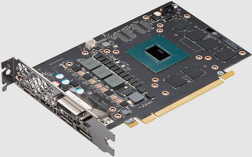
High-Density Interconnect PCBs for GPUs
High-Layer Count HDI PCB
A GPU board is one of the most demanding use cases for hdi circuit boards. The design must combine fine-pitch BGA breakout, high-speed serial links, memory routing, high-current power delivery, clock distribution, thermal spreading, and assembly flatness in one structure.
A high-layer count hdi pcb is usually required when:
- The GPU package has 0.5 mm, 0.4 mm, or smaller effective breakout pitch.
- PCIe Gen4, Gen5, Gen6, or other high-speed serial links need tight impedance control.
- Memory devices require short, length-controlled routing.
- VRM zones need multiple current paths and dense decoupling.
- Large BGA packages need controlled flatness after reflow.
- The enclosure requires shorter routing and reduced board area.
Typical GPU board ranges:
| GPU Board Type | Typical Layer Count | HDI Structure | Main Engineering Driver |
|---|---|---|---|
| Compact GPU module | 10-14 layers | 1+N+1 or 2+N+2 | BGA escape and memory routing |
| Graphics card PCB | 12-18 layers | Multi-stage HDI | GPU, memory, PCIe, power rails |
| AI GPU accelerator | 18-30 layers | 2+N+2, 3+N+3, or ELIC | High pin count and high-speed fabric |
| GPU server board | 24-36+ layers | High-layer HDI hybrid | PCIe, retimers, power, thermal copper |
| Ultra HDI GPU module | 16-30+ layers | UHDI or substrate-like routing | Ultra-fine pitch and dense fanout |
IPC-2226 establishes design requirements and considerations for high density interconnect printed boards, while IPC-2221 provides general printed board design requirements. IPC-6012 covers qualification and performance requirements for rigid printed boards, including multilayer boards that may contain blind or buried vias.
Characteristics of GPU HDI PCBs
GPU HDI PCBs normally include several technical features in the same board:
- 75/75 micron standard HDI trace and space.
- 50/50 micron advanced fine line routing in BGA escape zones.
- 75-100 micron laser microvias.
- 150-200 micron mechanical vias for non-dense regions.
- 200-300 micron microvia capture pads, depending on registration capability.
- Via-in-pad plated over for fine-pitch GPU BGA pads.
- 2+N+2, 3+N+3, ELIC, or Ultra HDI structures.
- Controlled impedance for 50 ohm, 85 ohm, 90 ohm, and 100 ohm channels.
- Low-loss laminate for long high-speed paths.
- Copper balance and warpage control around large BGA packages.
A design can pass CAD DRC and still fail fabrication review if the stackup, lamination cycles, material movement, microvia filling, solder mask registration, and reflow warpage are not checked together.
Megtron Material Selection
Why Megtron Matters
Megtron materials are selected for GPU hdi pcb fabrication when the loss budget is too tight for general FR-4. GPU boards often route high-speed serial links through long channels, connectors, retimers, memory zones, and BGA escape fields. The laminate’s Dk, Df, copper roughness, Tg, CTE, and thermal stability directly affect insertion loss, impedance, skew, reflow reliability, and production yield.
For a PCB factory engineer, the correct question is not “Which Megtron is the best?” It is:
- Which channels actually need ultra-low-loss material?
- Which layers need Megtron and which can use standard high-Tg material?
- Does the selected resin system survive the lamination count?
- Can the fabricator stock the selected glass style and copper foil?
- Does the impedance coupon match the real GPU routing geometry?
- Has the selected material been validated through reflow, thermal cycling, and microsection?
Megtron 6 to Megtron 10 Parameter Table
| Material | Public Parameter Snapshot | Typical GPU Use | Engineering Decision |
|---|---|---|---|
| Megtron 6 | Dk 3.34, Df 0.0037 @13 GHz, Tg 185°C, T288 with copper >120 min, peel strength 0.8 kN/m for 1 oz copper | PCIe Gen4 / Gen5 class GPU routing where loss budget allows | Good balance of loss, availability, HDI performance, and cost |
| Megtron 7 | Dk 3.37-3.63 depending on glass style; Df 0.001-0.002 @1 GHz; some models show Dk 3.31-3.61 and Df 0.002-0.003 @12-14 GHz; Tg around 200°C | Higher-speed GPU server boards, routers, large data-volume accelerator boards | Stronger loss performance than Megtron 6, but cost and availability must be confirmed early |
| Megtron 8 | Dk 3.08-3.22 @14 GHz; Df 0.0012-0.0016 @14 GHz; Tg DMA around 220°C; T288 with copper >60 min or >120 min by model | Ultra-low-loss GPU and AI accelerator channels with tight insertion-loss budgets | Better for very high-speed links, but requires supplier process qualification |
| Megtron 9 | Public material positioning targets the 224 Gbps generation; detailed Dk / Df values should be confirmed from current supplier datasheets | Next-generation GPU server, AI fabric, 224G-class channel planning | Do not lock material until supplier provides stackup, glass style, copper foil, and coupon data |
| Megtron 10 | No stable public parameter set was found from a verifiable official source at writing time | Future-class or customer-specific advanced GPU designs | Treat as a supplier-qualified material, not a fixed public specification |
Megtron 6 is described as an ultra-low-loss, highly heat-resistant multilayer material with excellent HDI and thermal performance; official data lists Dk and Df values around 3.34 and 0.0037 at 13 GHz for one low-Dk glass-cloth version. Megtron 8 official data shows lower Dk / Df at 14 GHz than Megtron 6 / 7 families, which explains why it is considered for more demanding high-speed network and accelerator use cases.
Material Selection Rules
GPU hdi pcb material selection should be based on the channel budget, not brand preference.
Use this selection logic:
- Use Megtron 6 when the channel length, connector count, and PCIe generation allow a moderate ultra-low-loss material.
- Use Megtron 7 when the design needs lower loss, better high-speed margin, or higher thermal stability.
- Use Megtron 8 when insertion loss, crosstalk, and higher-speed fabric margin dominate cost.
- Treat Megtron 9 as a 224G-class material path that requires supplier confirmation.
- Treat Megtron 10 as a qualification item unless the supplier provides current datasheet and process data.
- Avoid using the highest-cost material across all layers when only 4-8 signal layers need low-loss performance.
A mixed-material stackup can reduce cost, but it increases lamination risk. The fabricator must validate resin flow, CTE mismatch, drill quality, copper adhesion, and registration before production.
Signal Integrity and Power Delivery
Signal Integrity
Signal integrity in a GPU HDI PCB is controlled by impedance, loss, crosstalk, return path continuity, via transition quality, copper roughness, dielectric stability, and reflow-induced geometry change. HDI helps SI only when it shortens paths and removes unnecessary stubs. It hurts SI when microvias, split planes, and dense routing create discontinuities.
Practical SI targets:
| Interface | Common Target | Factory Control |
|---|---|---|
| PCIe differential pair | 85 ohm | Impedance coupon, low-loss material, via transition control |
| USB differential pair | 90 ohm | Pair spacing, skew, solder mask model |
| Ethernet / LVDS pair | 100 ohm | Plane continuity and trace geometry |
| Clock line | 50 ohm | Clean reference and isolation |
| RF control line | 50 ohm | Low-loss path and shielding clearance |
GPU SI review should include:
- Insertion loss budget by channel.
- Return loss and via discontinuity review.
- Backdrill or microvia strategy for stub reduction.
- Differential skew and intra-pair spacing.
- Reference plane continuity below high-speed layers.
- Glass weave and fiber effect review for long channels.
- Copper roughness model in the field solver.
Power Delivery
GPU boards have high current density and low-voltage rails. The PCB must support fast transient current without excessive voltage ripple or local heating.
Power delivery controls:
- Use multiple power and ground planes.
- Avoid neck-downs under GPU BGA escape regions.
- Use dense via arrays for GPU core rails.
- Keep decoupling loops short.
- Place high-frequency capacitors within 1-3 mm of critical power pins where possible.
- Use larger vias for high-current rails when routing density allows.
- Validate ripple under workload, not only at power-on.
- Simulate PDN impedance and verify with measurement.
| Power Item | Practical Range | Reason |
|---|---|---|
| Power via diameter | 0.20-0.30 mm | Better plating and current margin |
| Thermal via pitch | 0.50-1.00 mm | Improves heat spreading |
| Plane copper | 18-35 microns common | Balances current and fine etching |
| Decoupling distance | 1-3 mm near critical pins | Reduces loop inductance |
| Ripple target | Often below 3-5% of rail voltage | Protects GPU stability |
Thermal Management and Warpage
Thermal Management
GPU HDI boards generate heat from the GPU package, memory, VRM phases, retimers, clock ICs, and high-speed transceivers. Thermal design must be integrated into the hdi pcb structure, not left only to the heatsink.
Thermal controls include:
- Copper spreading under GPU and VRM zones.
- Thermal via arrays under hot components.
- Balanced copper distribution across layers.
- High-Tg resin system.
- Controlled board thickness.
- Reflow profile matched to board mass.
- Mechanical support under large packages.
- Warpage inspection after reflow simulation.
Typical production checks:
| Thermal Item | Practical Target | Factory Value |
|---|---|---|
| Board warpage | Below 0.75% diagonal target after reflow | Protects BGA solder joints |
| Thermal cycling | -40°C to 85°C, 100-500 cycles | Screens microvia and lamination weakness |
| Reflow simulation | 3-5 cycles for validation builds | Checks material and BGA stability |
| Cross-section | After thermal stress where needed | Confirms via and plating reliability |
| X-ray | BGA and VIPPO areas | Finds hidden solder and via defects |
Warpage Control
Warpage is a major GPU PCB manufacturing risk because GPU packages are large, copper distribution is uneven, and the stackup often has many layers.
Warpage reduction methods:
- Keep stackup symmetrical.
- Balance copper in opposing layers.
- Avoid large solid copper islands on only one side.
- Add copper thieving where it does not affect impedance.
- Use proper bake and lamination control.
- Avoid placing heavy heatsink pressure directly on unsupported BGA corners.
- Check flatness before and after reflow.
A small warpage difference may not show in bare-board E-test, but it can create corner solder joint stress, intermittent memory errors, or PCIe link instability after thermal soak.
HDI Structure Types
Multi-Stage HDI
Multi-stage HDI uses sequential buildup layers. A 2+N+2 board has two buildup layers on each side of a core. A 3+N+3 board has three buildup layers on each side. Each stage adds dielectric, laser drilling, copper plating, imaging, etching, and registration control.
| HDI Structure | Best Use | Cost / Risk Level |
|---|---|---|
| 1+N+1 | Moderate GPU control board | Lower HDI cost |
| 2+N+2 | Graphics card and GPU module | Higher density and cost |
| 3+N+3 | AI GPU accelerator | More process control required |
| ELIC | Extreme GPU BGA density | Highest routing freedom and cost |
| Ultra HDI | Sub-30 micron routing and dense fanout | Limited supplier base and tight metrology |
ELIC
ELIC means Every Layer Interconnection. In an ELIC structure, each layer can connect to adjacent layers through copper-filled microvias. This gives the designer free interconnection between layers and supports dense GPU routing where standard staged HDI may not provide enough escape channels.
ELIC benefits:
- Free interconnection between adjacent layers.
- Stacked copper-filled microvias.
- Higher routing density.
- Shorter escape paths.
- More flexible power and signal layer access.
- Better package breakout for high-pin-count GPUs.
- Potential layer-count reduction when routing is extremely congested.
ELIC risks:
- More lamination cycles.
- More copper-filled microvia process steps.
- More microsection inspection.
- Higher risk from stacked via fatigue.
- Higher cost and longer lead time.
- Narrower supplier base.
Ultra HDI Technology
Characteristics and Technical Specs
Ultra High-Density Interconnect technology pushes below standard HDI geometries. It is relevant for future GPU boards, AI modules, chiplet-related designs, and substrate-like fanout regions.
| Feature | Standard HDI | Ultra HDI |
|---|---|---|
| Trace width / spacing | 75/75 to 50/50 microns | Below 30/30 microns, sometimes near 20 microns |
| Microvia diameter | 75-100 microns | 50-75 microns in advanced builds |
| Dielectric thickness | 50-80 microns | 25-50 microns |
| Fabrication method | Laser drill, plate, sequential lamination | Advanced imaging, mSAP-like or advanced subtractive control |
| Main use | GPU BGA breakout and high-speed boards | Ultra-fine pitch, chiplet-style fanout, advanced modules |
Ultra HDI provides high-density component placement, improved signal integrity, increased functionality, shorter interconnects, and potential layer-count reduction. It should be selected only when standard HDI cannot meet fanout or layer targets.
Applications and Industry Adoption
Ultra HDI adoption is strongest in:
- High-performance computing
- GPU accelerator boards
- AI server modules
- Chiplet-related hardware
- Advanced networking
- Medical electronics
- Automotive technology
- Aerospace modules
- Compact consumer electronics
The production challenge is metrology. As line width moves below 30 microns, imaging control, etch uniformity, copper thickness, panel cleanliness, and defect inspection become more critical.
Benchuang Electronics
GPU HDI Manufacturing Fit
Benchuang Electronics should be positioned as a high-end HDI and multilayer PCB manufacturer for customers who need dense routing, high-layer-count boards, hdi pcb prototype support, and production-oriented engineering review. Public company information describes Benchuang as founded in 2007, with a 40,000 square meter facility, nearly 500 employees, and annual HDI production capacity stated at 480,000 square meters. It also presents high-end HDI and multilayer PCB manufacturing, DFM support, turnkey PCBA capability, and applications across mobile communications, automotive electronics, aerospace, IoT, industrial control, and security.
For GPU HDI PCB projects, Benchuang Electronics should be evaluated by engineering evidence rather than general capability wording:
- 50/50 micron and 75/75 micron routing capability.
- Laser microvia diameter and registration records.
- Copper-filled stacked microvia control.
- VIPPO dimple and planarization criteria.
- 2+N+2 and 3+N+3 lamination experience.
- Impedance coupon reports for 50, 85, 90, and 100 ohm nets.
- Warpage data after reflow.
- X-ray and microsection records.
- PVT yield history.
Factory Review Value
A qualified hdi pcb manufacturer for GPU hardware should ask these questions before final quotation:
- What is the GPU package pitch?
- Which nets need 85 ohm PCIe control?
- Which layers require Megtron 6, 7, 8, or higher-grade materials?
- Does the board need ELIC or only multi-stage HDI?
- Are stacked microvias required under the GPU?
- What VIPPO dimple limit is acceptable?
- What is the maximum warpage after reflow?
- Which rails carry peak current?
- Where are the thermal via arrays?
- Will PCA testing include workload-level thermal and link training tests?
This type of review prevents the common mistake of quoting a GPU hdi pcb only from Gerber files without understanding SI, PI, and assembly risk.
Two Key Comparisons
Multi-Stage HDI vs ELIC
| Item | Multi-Stage HDI | ELIC |
|---|---|---|
| Routing freedom | Good | Highest |
| Cost | High | Very high |
| Lamination demand | Medium to high | Very high |
| Best use | GPU boards with controlled density | Extreme BGA and every-layer access |
| Reliability control | Manageable with strong DFM | Requires strict microvia fill validation |
| Supplier base | Wider | Narrower |
Megtron 6 vs Megtron 8 / 9 / 10 Class
| Item | Megtron 6 Class | Megtron 8 / 9 / 10 Class |
|---|---|---|
| Loss performance | Ultra-low loss | Ultra-low to next-generation low loss |
| Public parameter certainty | Strong for Megtron 6 | Strong for Megtron 8, partial for Megtron 9, limited for Megtron 10 |
| Cost | Lower | Higher |
| Availability | Broader | Must confirm early |
| Best use | Many GPU and PCIe boards | Highest-speed GPU and AI channels |
| Fabrication risk | More familiar | Requires process qualification |
Real Factory Case
GPU Accelerator Board
A customer released a GPU hdi pcb prototype for an accelerator board with one large GPU BGA, eight memory packages, PCIe edge interface, VRM sections, clock ICs, retimers, and high-current power planes.
| Item | Project Data |
|---|---|
| Board type | GPU HDI PCB |
| Layer count | 20 layers |
| HDI structure | 3+14+3 |
| Board thickness | 1.8 mm |
| Material | Mixed low-loss high-Tg laminate |
| Trace / space | 50/50 microns in GPU escape |
| Microvia | 75 microns, copper filled |
| Via type | Stacked microvia and VIPPO |
| Impedance | 85 ohm PCIe, 100 ohm differential, 50 ohm clock |
| Finish | ENIG |
| Quality control | AOI, E-test, X-ray, microsection, impedance coupon |
Problems Found
The first EVT build used 100 boards. Bare-board E-test passed, but system test found:
- PCIe training failures on 8 boards.
- GPU corner BGA solder variation on X-ray.
- VRM hotspot above 95°C.
- Board warpage above target after reflow.
- Two boards with intermittent memory errors after thermal soak.
Root causes:
- One PCIe lane crossed a reference discontinuity near a microvia transition.
- VIPPO dimple variation reached 16 microns in one BGA region.
- Copper imbalance around VRM layers increased local warpage.
- Power via count under one VRM phase was too low.
- One high-speed layer used a material substitution without updated impedance coupon data.
Improvement Result
Corrective actions included adding ground stitching, changing two stacked microvia columns to staggered structures, reducing VIPPO dimple target below 10 microns, rebalancing copper on two internal layers, increasing VRM via count from 32 to 64, and locking material by impedance coupon data.
| Metric | EVT Result | Revised Pilot |
|---|---|---|
| PCIe training failures | 8/100 | 0/180 |
| VRM hotspot | 95°C | 83°C |
| VIPPO dimple range | 8-16 microns | Below 10 microns |
| Memory thermal errors | 2/100 | 0/180 |
| First-pass system yield | 86.0% | 97.2% |
This case shows why GPU HDI PCB development must connect stackup, Megtron material selection, SI, power delivery, thermal control, microvia reliability, VIPPO quality, and PCA functional testing.
Common Design Errors
Layout Errors
- Choosing ELIC when 2+N+2 can route the design.
- Using stacked microvias everywhere instead of only under dense GPU escape zones.
- Routing PCIe lanes across split reference planes.
- Reducing trace width without recalculating impedance.
- Leaving no impedance coupons for critical channels.
- Placing decoupling capacitors too far from GPU power pins.
- Ignoring current density in BGA power escape areas.
Fabrication Errors
- Specifying VIPPO without dimple and cap limits.
- Choosing Megtron 8 or future-grade material without confirming stock and process window.
- Mixing materials without checking CTE and lamination behavior.
- Using thick copper in ultra-fine routing regions.
- Ignoring copper balance under large GPU packages.
- Skipping microsection for stacked microvias.
- Treating hdi pcb prototype success as proof of mass production readiness.
Assembly and PCA Errors
- Not checking warpage after reflow.
- Not X-raying BGA and VIPPO regions.
- Not validating heatsink pressure on GPU corners.
- Not measuring voltage ripple under GPU workload.
- Not separating PCB fabrication test from PCA functional validation.
- Not testing PCIe link training at temperature.
PCB is the bare printed circuit board. PCA is the assembled circuit board with components, solder joints, firmware, labels, inspection records, and functional test data. A GPU hdi pcb may pass bare-board testing while the PCA fails because of BGA voids, heatsink pressure, power ripple, or high-speed channel margin.
FAQ About HDI PCB for GPU
Question: Why do GPUs need HDI PCB?
Answer: GPUs need HDI PCB because high-pin-count BGA packages, memory devices, PCIe lanes, high-current power rails, and thermal constraints require more routing density than a standard PCB can provide. Microvias, via-in-pad, sequential lamination, and fine-line routing help escape dense GPU packages and shorten critical signal paths.
Question: Which Megtron material should be used for GPU HDI PCB?
Answer: The material should be chosen by insertion-loss budget, PCIe generation, channel length, connector count, copper roughness, and supplier process capability. Megtron 6 can fit many GPU designs when the loss budget allows. Megtron 7 and Megtron 8 offer lower-loss options for more demanding channels. Megtron 9 or Megtron 10 class materials should be locked only after supplier datasheet, coupon, and process qualification are confirmed.
Question: What is ELIC in GPU HDI PCB design?
Answer: ELIC means Every Layer Interconnection. It allows adjacent layers to connect through copper-filled microvias across the board stack. ELIC gives engineers more freedom for GPU BGA escape and dense high-speed routing, but it increases cost, lamination complexity, microvia fill requirements, and inspection demand.
Question: How should engineers choose PCB type for GPU hardware?
Answer: Engineers should choose PCB type by package pitch, routing density, interface speed, loss budget, power density, thermal path, and production volume. A standard multilayer PCB may fit low-density control designs. A high density interconnect board fits dense GPU modules. Ultra HDI or ELIC should be used only when standard HDI cannot meet fanout, layer count, or SI targets.


![Understanding PCB Costs & Pricing [Your Complete Guide]](https://hdicircuitboard.com/wp-content/uploads/elementor/thumbs/Understanding-PCB-Costs-Pricing-Your-Complete-Guide-qzzhe6mcaxuolkux3xalfktgavumi9y1aqfbs9bpv4.webp "Understanding PCB Costs & Pricing [Your Complete Guide]")


