
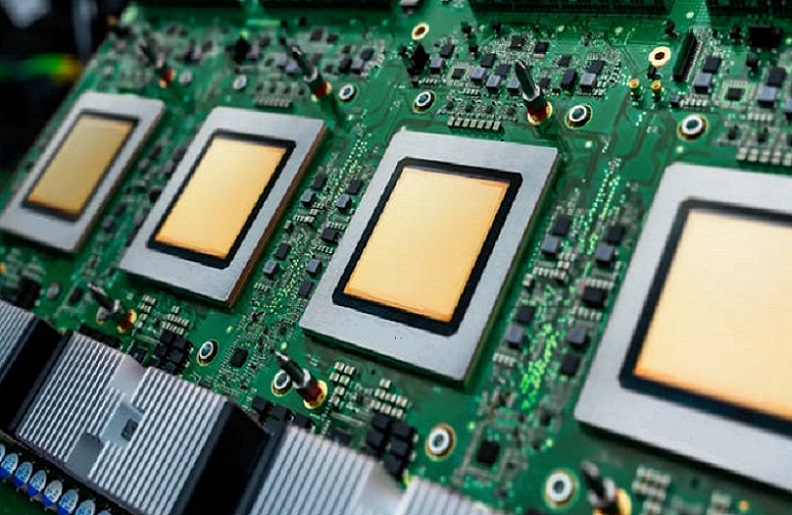
HDI PCB for TPU hardware uses high density interconnect structures, high-layer count stackups, low Dk materials, microvias, via-in-pad, sequential lamination, controlled impedance, dense power distribution, and thermal management to support Tensor Processing Units in cloud accelerators, Edge TPU modules, embedded AI systems, and high-performance computing platforms. For engineers, the value of an hdi pcb is not only smaller routing area. It is the ability to route high-pin-count TPU packages, reduce via stubs, improve signal integrity, stabilize power delivery, manage heat, and move from hdi pcb prototype to repeatable hdi pcb fabrication with controlled yield.
HDI PCBs for TPUs
Layer Count and Density
High-Density Interconnect PCBs for Tensor Processing Units must support dense package breakout, high-speed interconnects, memory interfaces, power rails, clocks, test access, and thermal structures in limited board space. A TPU system can range from a small Edge TPU module to a high-layer accelerator board used in data centers.
| TPU Hardware Type | Typical PCB Structure | HDI Requirement | Main Engineering Driver |
|---|---|---|---|
| Edge TPU module | 6-10 layers | 1+N+1 or compact HDI | Miniaturization and low power |
| Embedded TPU carrier | 8-14 layers | Microvias, controlled impedance | Connector, memory, camera, sensor routing |
| Cloud TPU accelerator | 16-30 layers | 2+N+2, 3+N+3, or ELIC | High pin count, power, high-speed I/O |
| HPC TPU board | 20-36+ layers | High-layer count hdi pcb | Data center performance and interconnect density |
| Future TPU module | Ultra HDI or substrate-like PCB | Sub-30 micron routing | Dense package and heterogeneous integration |
IPC-2226 establishes design requirements and considerations for HDI printed boards and microvia technology, while IPC-2221 provides generic printed board design requirements. IPC-6012 covers qualification and performance requirements for rigid printed boards, including multilayer boards with blind and buried vias.
Key Technical Characteristics
Key technical characteristics of HDI PCBs for TPUs include:
- Trace / space: 75/75 microns for standard HDI, 50/50 microns for advanced TPU escape regions
- Ultra HDI routing: below 30/30 microns where supplier capability supports it
- Microvia diameter: 75-100 microns for common laser-drilled HDI structures
- Advanced microvia: 50-75 microns for tighter Ultra HDI regions
- Dielectric thickness: 50-80 microns for common HDI buildup layers
- Low Dk dielectric: around Dk 3.0-3.8 depending on speed, material family, and stackup
- Impedance: 50 ohm single-ended, 85 ohm high-speed differential, 90 ohm USB, 100 ohm Ethernet or LVDS
- Surface finish: ENIG, immersion silver, or other fine-pitch compatible finish
- Test: AOI, E-test, X-ray, microsection, impedance coupon, and thermal cycling where required
TPU Systems and PCB Role
Cloud TPUs and Edge TPU
Cloud TPUs are built for large-scale AI training and inference, while Edge TPU hardware is built for compact embedded inference. TPU v5p is an official Cloud TPU generation with 3D torus connectivity for larger slices, and earlier TPU v4 research describes 4096-chip supercomputer scale with optical circuit switching. More recent public reporting describes eighth-generation TPU 8t and TPU 8i as separate training and inference chips, but engineers should verify current hardware documentation before using these names in product requirements.
The PCB role changes by TPU class:
- Cloud TPU boards prioritize data center performance, power density, interconnect bandwidth, thermal path, and high-layer count.
- Edge TPU boards prioritize miniaturization, energy efficiency, camera or sensor connectivity, memory routing, and embedded applications.
- Embedded TPU carriers prioritize power integrity, connector reliability, mechanical fit, and manufacturable stackup.
- Future TPU designs may require finer line widths, denser fanout, lower-loss material, and tighter integration between package and PCB.
Key Components of a TPU PCB
A TPU PCB normally integrates:
- TPU ASIC or accelerator package
- Memory devices or memory interface routing
- Power management ICs and VRM stages
- Clock generators and reset circuits
- High-speed connectors or board-to-board interfaces
- Ethernet, PCIe, USB, MIPI, or proprietary links
- Temperature sensors and telemetry circuits
- Flash or boot memory
- Test pads, programming access, and boundary scan support
- Thermal vias, copper spreading, and mechanical mounting features
The factory must treat these as a connected system. A bare hdi circuit board can pass electrical test while the assembled PCA fails because of BGA voiding, PMIC heating, clock noise, connector stress, or impedance drift.
Materials and Stackup
Low Dk HDI PCB Materials
Low Dk HDI PCB materials reduce propagation delay and help control impedance in dense high-speed routing. Low Df materials reduce insertion loss, which is critical when TPU boards include long interconnects, high-speed connectors, retimers, memory links, or data center fabric routes.
| Material Item | Practical Range | TPU PCB Value |
|---|---|---|
| Dk | 3.0-3.8 common for many high-speed laminates | Controls impedance and propagation delay |
| Df | Below 0.005 for demanding high-speed channels | Reduces insertion loss |
| Tg | 170 C or higher preferred | Improves reflow and thermal cycling margin |
| Copper roughness | Low-profile copper preferred | Reduces conductor loss |
| Build-up dielectric | 25-80 microns | Enables laser microvias |
| Copper thickness | 9-18 microns for fine routing, 35 microns for power regions | Balances density and current |
The practical rule is to use low-loss material where the signal budget requires it, not everywhere. A mixed stackup can reduce cost, but the hdi pcb manufacturer must validate lamination flow, CTE mismatch, registration, and impedance coupons.
Typical Stackup for TPU Accelerators
| Stackup Type | Typical Use | Cost and Risk |
|---|---|---|
| 1+N+1 | Edge TPU and compact modules | Lower cost, fewer lamination cycles |
| 2+N+2 | TPU carrier and moderate accelerator boards | Better breakout, higher registration control |
| 3+N+3 | Cloud TPU or HPC accelerator boards | Higher density, more lamination risk |
| ELIC | Every-layer routing under dense ASIC packages | Highest routing freedom and process demand |
| Ultra HDI | Sub-30 micron routing and substrate-like fanout | Advanced supplier capability required |
A high-layer count hdi pcb should not be selected only to solve routing congestion late in layout. The stackup should be planned before TPU BGA escape, memory routing, power rail definition, and impedance modeling.
Microvia and Fabrication
Advanced Drilling and Alignment
Microvia technology is central to hdi pcb fabrication for TPUs. It allows the design to escape dense BGA fields without using large through vias that consume routing channels.
Factory control points:
- Laser microvia diameter: 75-100 microns for stable HDI production
- Advanced microvia diameter: 50-75 microns for tighter Ultra HDI regions
- Microvia aspect ratio: normally kept at or below 1:1
- Capture pad: commonly 200-300 microns depending on registration capability
- Stacked microvias: require copper filling and strict inspection
- Staggered microvias: often lower risk and lower cost when space allows
- Alignment: registration must be checked after every sequential lamination cycle
Sequential Lamination and SBU
Sequential lamination, also called SBU in many HDI contexts, builds the board in stages. Each cycle adds dielectric, laser drilling, plating, imaging, etching, and registration risk.
Process sequence:
- Build and inspect the inner core.
- Drill and plate buried vias where required.
- Laminate the first buildup dielectric.
- Laser drill microvias.
- Plate or copper fill microvias.
- Image and etch the buildup copper.
- Repeat for 2+N+2, 3+N+3, or ELIC structures.
- Add finish, solder mask, impedance coupons, and final test.
- Inspect with AOI, E-test, X-ray, and microsection.
Sequential lamination improves density, but it increases cost and yield risk. Each lamination stage can introduce dimensional movement.
Signal and Power Design
Signal Integrity
Signal integrity in TPU HDI PCBs is controlled by impedance, return path, insertion loss, crosstalk, via transition quality, differential skew, copper roughness, and dielectric stability.
| Interface | Common Target | Factory Control |
|---|---|---|
| PCIe or high-speed fabric | 85 ohm differential | Coupon test, via model, material loss check |
| USB | 90 ohm differential | Pair spacing, skew, solder mask model |
| Ethernet / LVDS | 100 ohm differential | Plane continuity and geometry |
| Clock lines | 50 ohm single-ended | Clean reference and isolation |
| RF or telemetry control | 50 ohm single-ended | Low-loss path and shielding clearance |
HDI improves signal integrity when it shortens routes, reduces via stubs, and keeps high-speed paths close to stable reference planes. It creates new risk when microvias are placed without return-path planning.
Power Distribution
TPU boards can carry high current at low voltage. The PCB must deliver fast transient current without voltage droop, excessive ripple, or local heating.
Power distribution controls:
- Use multiple power and ground planes.
- Avoid plane neck-downs under the TPU BGA.
- Add via arrays for low-inductance power transfer.
- Place decoupling within 1-3 mm of critical power pins where possible.
- Use larger mechanical vias for high-current regions when density allows.
- Simulate PDN impedance before layout release.
- Measure rail ripple under real inference or training workload.
| Power Item | Practical Target | Reason |
|---|---|---|
| Power via diameter | 0.20-0.30 mm | Better plating and current margin |
| Decoupling distance | 1-3 mm near critical pins | Lower loop inductance |
| Plane copper | 18-35 microns common | Balances current and fine routing |
| Ripple target | Often below 3-5% of rail voltage | Protects accelerator stability |
| Thermal via pitch | 0.50-1.00 mm | Improves heat spreading |
Thermal Management
Thermal Reliability
Thermal management is not only heatsink design. In TPU hardware, the hdi pcb must transfer heat, survive reflow, maintain BGA flatness, and protect microvia reliability.
Thermal controls:
- Copper spreading under TPU and PMIC zones
- Thermal via arrays under hot components
- Balanced copper distribution to reduce warpage
- High Tg or low-loss material with proper thermal stability
- Reflow profile matched to thick high-layer boards
- X-ray for BGA and via-in-pad areas
- Thermal cycling for reliability lots
| Thermal Item | Practical Target | Factory Value |
|---|---|---|
| Board warpage | Below 0.75% diagonal target after reflow | Protects BGA solder joints |
| Thermal cycling | -40 C to 85 C, 100-500 cycles | Screens microvia and lamination weakness |
| Reflow simulation | 3-5 cycles for validation builds | Checks material and BGA stability |
| Cross-section | After thermal stress where needed | Confirms via and plating reliability |
| X-ray | BGA and VIPPO areas | Finds hidden solder and via defects |
Structural Integrity
Structural integrity depends on layer symmetry, copper balance, resin stability, hole plating, and mechanical support. TPU boards often include large packages and high-current regions, so warpage and local stress must be checked before mass production.
Heterogeneous Integration
Role in AI Infrastructure
TPU hardware fits into AI infrastructure through modules, carrier boards, server boards, interconnect fabrics, and embedded inference systems. Heterogeneous integration pushes more compute, memory, power, and communication into smaller assemblies.
This increases demand for:
- High density interconnect routing
- Low-loss materials
- Thin dielectric buildup
- Dense microvia fanout
- Power delivery close to accelerator packages
- Higher component density
- Stronger inspection and traceability
Future Interconnects
Future interconnects may involve tighter package-to-board transitions, chiplet-related routing, optical or copper fabric, glass substrate discussion, and Ultra HDI structures. The PCB may need to act more like a bridge between package substrate, system board, power module, and thermal structure.
Top Manufacturing Trends
Supply Chain Localization
Supply chain localization is becoming more important for TPU and AI accelerator hardware because high-layer boards, HDI materials, low-loss laminates, copper foils, specialty finishes, and assembly capacity all affect project schedule. Localized or regionalized supply reduces risk when prototype, DVT, PVT, and mass production need faster engineering feedback.
Key localization factors:
- HDI material inventory
- Laser drilling capacity
- Sequential lamination capacity
- Low-loss laminate qualification
- X-ray and microsection capability
- Local DFM support
- Assembly and test fixture support
- PCN and EOL management
Key Suppliers
Benchuang Electronics should be introduced as a high-end HDI and multilayer PCB manufacturer for dense hdi circuit boards, industrial AI hardware, communication products, automotive electronics, and turnkey PCBA projects. Public company information describes Benchuang as founded in 2007, with high-end HDI and multilayer PCB manufacturing focus, DFM support, turnkey PCBA capability, and annual HDI production capacity stated at 480,000 square meters.
For TPU HDI PCB projects, Benchuang Electronics should be evaluated by engineering evidence:
- 50/50 micron and 75/75 micron routing capability
- Laser microvia diameter and registration reports
- Copper-filled stacked microvia control
- VIPPO dimple and planarization criteria
- 2+N+2 and 3+N+3 lamination experience
- Impedance coupon reports for 50, 85, 90, and 100 ohm nets
- Warpage data after reflow
- X-ray and microsection records
- hdi pcb prototype to PVT yield history
Key Benefits
Miniaturization and Energy Efficiency
HDI PCB benefits for TPU hardware include:
- Smaller board outline
- Higher density under TPU packages
- Reduced via stub
- Shorter signal path
- Lower parasitic inductance in power delivery
- Better decoupling placement
- Lower connector count
- More compact embedded AI modules
Energy efficiency depends on the full system, but PCB design affects losses through PDN impedance, thermal resistance, signal loss, and connector count.
Enhanced Reliability
Enhanced reliability comes from design restraint, not maximum complexity. A reliable hdi pcb for TPU hardware uses HDI only where density requires it, keeps power routing robust, verifies signal integrity, controls material movement, validates via structures, and tests the assembled PCA under workload.
Two Key Comparisons
Cloud TPU PCB vs Edge TPU PCB
| Item | Cloud TPU PCB | Edge TPU PCB |
|---|---|---|
| Main priority | Data center performance | Miniaturization and power efficiency |
| Layer count | 16-36+ layers | 6-12 layers |
| HDI need | High-layer HDI, ELIC, or 3+N+3 | 1+N+1 or compact HDI |
| Power density | Very high | Moderate to low |
| Thermal design | Heatsink, cold plate, system airflow | Small enclosure and local heat spreading |
| Best use | HPC and large-scale AI infrastructure | Embedded applications and compact inference |
Standard HDI vs Ultra HDI
| Item | Standard HDI | Ultra HDI |
|---|---|---|
| Trace / space | 75/75 to 50/50 microns | Below 30/30 microns |
| Microvia diameter | 75-100 microns | 50-75 microns in advanced builds |
| Dielectric thickness | 50-80 microns | 25-50 microns |
| Cost | High | Very high |
| Supplier base | Broader | Narrower |
| TPU use case | Most dense TPU carrier boards | Future package fanout and advanced modules |
Real Factory Case
TPU Accelerator Board
A customer released an hdi pcb prototype for a TPU accelerator carrier with one high-pin-count TPU package, four memory devices, PCIe interface, two PMIC zones, clock circuitry, flash memory, and a high-speed board-to-board connector.
| Item | Project Data |
|---|---|
| Board type | TPU accelerator HDI PCB |
| Layer count | 18 layers |
| HDI structure | 3+12+3 |
| Board thickness | 1.6 mm |
| Material | Low Dk, low-loss high-Tg laminate |
| Trace / space | 50/50 microns in TPU escape |
| Microvia | 75 microns, copper filled |
| Via type | Stacked microvia and VIPPO |
| Impedance | 85 ohm high-speed differential, 100 ohm differential, 50 ohm clock |
| Finish | ENIG |
| Inspection | AOI, E-test, X-ray, impedance coupon, microsection |
Production Problems
The first EVT build used 80 boards. Bare-board E-test passed, but system testing found:
- High-speed link training failures on 5 boards
- TPU rail ripple above target during workload bursts
- PMIC hotspot above 91 C
- One BGA corner with unstable X-ray void profile
- Two boards with intermittent memory errors after thermal soak
Root causes:
- One high-speed pair crossed a reference discontinuity near a microvia transition.
- Power via count under the PMIC was too low.
- VIPPO dimple variation reached 14 microns in one TPU BGA zone.
- Copper imbalance near the PMIC increased local warpage.
- One low Dk material substitution changed impedance coupon results.
Corrective Actions
The factory and layout team changed:
- Added ground stitching near the high-speed transition.
- Increased PMIC power via count from 28 to 56.
- Reduced VIPPO dimple target below 10 microns.
- Rebalanced copper on two internal layers.
- Locked laminate and glass style before pilot build.
- Added X-ray sampling for every panel.
- Added microsection samples from stacked microvia fields.
| Metric | EVT Result | Revised Pilot |
|---|---|---|
| Link training failures | 5/80 | 0/160 |
| PMIC hotspot | 91 C | 80 C |
| TPU rail ripple | 4.8% | 2.1% |
| BGA void variation | Unstable | Stable X-ray profile |
| First-pass system yield | 88.8% | 97.5% |
This case shows why TPU hdi pcb fabrication must connect stackup, SI, power distribution, material control, thermal behavior, microvia reliability, VIPPO quality, and PCA workload testing.
Common Design Errors
Layout Errors
- Choosing ELIC when 2+N+2 can route the design
- Using stacked microvias everywhere instead of only where density requires it
- Routing high-speed pairs across split reference planes
- Reducing trace width without recalculating impedance
- Leaving no impedance coupons for critical channels
- Placing decoupling capacitors too far from TPU power pins
- Ignoring current density in BGA power escape areas
Fabrication Errors
- Specifying VIPPO without dimple and cap limits
- Choosing low Dk material without confirming stock and process window
- Mixing materials without checking CTE and lamination behavior
- Using thick copper in ultra-fine routing regions
- Ignoring copper balance under large TPU packages
- Skipping microsection for stacked microvias
- Treating hdi pcb prototype success as proof of mass production readiness
Assembly and PCA Errors
- Not checking warpage after reflow
- Not X-raying BGA and VIPPO regions
- Not validating heatsink pressure on TPU corners
- Not measuring voltage ripple under AI workload
- Not separating PCB fabrication test from PCA functional validation
- Not testing high-speed links at temperature
PCB is the bare printed circuit board. PCA is the assembled circuit board with components, solder joints, firmware, labels, inspection records, and functional test data. A TPU hdi pcb may pass bare-board testing while the PCA fails due to BGA voiding, power instability, thermal stress, or signal integrity margin.
FAQ About HDI PCB for TPU
Question: Why do TPUs need HDI PCB?
Answer: TPUs need HDI PCB because high-pin-count accelerator packages, dense memory routing, high-speed interfaces, power rails, and thermal limits require more routing density than standard PCB technology can provide. Microvias, via-in-pad, sequential lamination, and fine-line routing help reduce board area and shorten critical paths.
Question: What layer count is common for TPU HDI PCB?
Answer: Edge TPU boards may use 6-12 layers, while cloud TPU accelerator boards often need 16-30+ layers depending on package pitch, memory interface, interconnect speed, power rail count, and thermal structure. ELIC or Ultra HDI should be used only when standard HDI cannot meet fanout or layer targets.
Question: What materials are used in TPU HDI PCB?
Answer: TPU HDI PCBs often use high-Tg FR-4, low Dk and low Df laminates, thin buildup dielectrics, low-profile copper, ENIG or immersion silver finish, and controlled impedance coupons. The material should be chosen by insertion loss, impedance stability, thermal reliability, and fabrication capability.
Question: How should engineers choose PCB type for TPU hardware?
Answer: Engineers should choose PCB type by TPU package pitch, routing density, signal speed, power density, thermal path, mechanical size, and production volume. Standard multilayer PCB can fit simple carriers. High density interconnect PCB fits dense TPU modules. Ultra HDI or ELIC should be reserved for extreme fanout and future advanced packages.


![Understanding PCB Costs & Pricing [Your Complete Guide]](https://hdicircuitboard.com/wp-content/uploads/elementor/thumbs/Understanding-PCB-Costs-Pricing-Your-Complete-Guide-qzzhe6mcaxuolkux3xalfktgavumi9y1aqfbs9bpv4.webp "Understanding PCB Costs & Pricing [Your Complete Guide]")


