







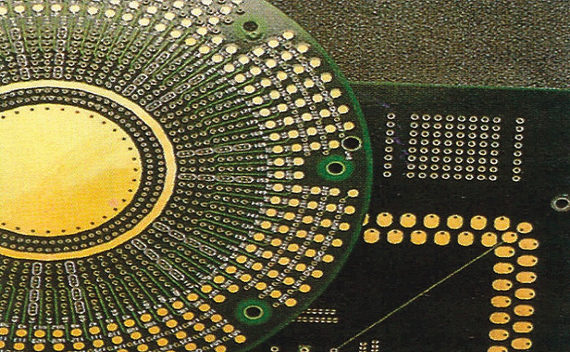
HDI PCB impedance control means designing and fabricating transmission lines so their characteristic impedance stays within a specified tolerance, usually ±10% for standard high-speed boards and ±5% for tighter designs. In a high density interconnect board, impedance is controlled by trace width, trace spacing, copper thickness, dielectric constant, dielectric thickness, reference planes, solder mask, microvias, blind or buried vias, sequential lamination, and copper plating. IPC-2141 defines controlled impedance as maintaining a specified tolerance in the characteristic impedance of an interconnect line used to connect different devices in high-speed digital or high-frequency analog circuits. (IPC-2141)
Impedance Control
What Impedance Control Means
Impedance control is the process of designing a PCB trace as a predictable transmission line. When signal rise time is fast enough, the trace no longer behaves like a simple wire. It behaves as a structure controlled by conductor geometry, dielectric thickness, material Dk, copper roughness, and return path.
Common controlled-impedance targets include:
| Signal Type | Common Target | Typical Use |
|---|---|---|
| Single-ended clock | 50 ohm | Clock, RF control, high-speed single-ended nets |
| USB differential | 90 ohm | USB 2.0, USB 3.x routing |
| Ethernet / LVDS | 100 ohm | Ethernet, LVDS, many differential links |
| PCIe differential | 85 ohm | PCIe Gen3, Gen4, Gen5 design families |
| DDR data / address | 40-60 ohm | Memory bus routing by controller requirement |
A controlled hdi pcb should define the target impedance, tolerance, routing layer, reference plane, material, copper thickness, and test coupon before hdi pcb fabrication begins.
Why HDI Changes the Problem
HDI boards are harder to control than conventional multilayer boards because routing is denser, dielectric layers are thinner, copper can be thinner in fine-line zones, and signals often transition through microvias or blind vias close to BGA pads.
HDI impedance control is affected by:
- 75/75 micron or 50/50 micron trace and space
- 25-80 micron build-up dielectric
- 9-18 micron copper for fine-line layers
- Laser microvias from 50-125 microns
- Via-in-pad under fine-pitch BGA
- Sequential lamination shrinkage
- Copper plating variation
- Solder mask over external microstrip traces
- Reference-plane gaps under dense fanout
IPC-2221 establishes generic requirements for printed board design, while IPC-6012 covers qualification and performance requirements for rigid printed boards, including multilayer boards with or without blind and buried vias. (IPC-2221, IPC-6012)
Design Rules
Trace Width and Spacing
Trace width is one of the most visible impedance variables, but it cannot be set alone. A 50 ohm line may need a different width depending on dielectric height, copper thickness, solder mask, and Dk.
Typical HDI planning values:
| Routing Condition | Trace / Space | Copper Thickness | Typical Use |
|---|---|---|---|
| Standard HDI routing | 75/75 microns | 12-18 microns | Compact digital routing |
| Fine BGA breakout | 50/50 microns | 9-12 microns | 0.4 mm or 0.5 mm BGA escape |
| High-speed microstrip | 75-125 micron trace | 12-18 microns | Outer-layer controlled impedance |
| High-speed stripline | 75-150 micron trace | 12-18 microns | Inner-layer controlled impedance |
| Power region | 150 microns or wider | 35 microns or higher | Current carrying, not fine impedance |
Fine-line HDI routing should avoid unnecessary thick copper. A 50/50 micron region on 35 micron copper is harder to etch consistently than the same geometry on 12 micron copper.
Dielectric Constant, Dk
Dielectric constant controls signal velocity and impedance. Lower Dk usually increases impedance for the same trace geometry, while higher Dk reduces impedance. The effective Dk also depends on whether the trace is microstrip, stripline, or embedded in build-up dielectric.
Common material planning ranges:
| Material Type | Typical Dk Range | Typical Use |
|---|---|---|
| Standard FR4 | 3.8-4.4 | General digital HDI |
| High-Tg FR4 | 3.7-4.2 | Industrial and lead-free assembly |
| Low-loss laminate | 3.0-3.7 | PCIe, RF, high-speed digital |
| Build-up dielectric | 3.1-3.8 | Microvia layers and fine fanout |
| PTFE-based material | 2.2-3.0 | RF and microwave circuits |
The hdi pcb manufacturer should use the laminate supplier’s Dk at the design frequency, not only the nominal 1 MHz data-sheet value.
Reference Planes
A controlled-impedance trace needs a clean return path. The reference plane is usually ground, but it can also be a stable power plane if decoupling and return path design support it.
Reference-plane rules:
- Keep a continuous reference under high-speed traces.
- Avoid routing across plane splits.
- Place stitching vias near layer changes.
- Keep differential pair return paths symmetrical.
- Avoid reference-plane voids under BGA escape regions.
- Do not use narrow copper islands as high-speed references.
- Define stripline and microstrip layers in the stack-up drawing.
HDI-Specific Challenges
Blind and Buried Vias
Blind and buried vias reduce routing blockage, but they can create impedance discontinuities if not modeled. A microvia is short, but the transition still has pad capacitance, anti-pad geometry, target pad effects, and return-current behavior.
| Via Structure | Impedance Effect | Design Control |
|---|---|---|
| Through via | Long stub and higher discontinuity | Backdrill or avoid on high-speed nets |
| Blind microvia | Shorter transition | Pad size and reference return control |
| Buried via | Internal transition | Anti-pad and reference-plane planning |
| Stacked microvia | Compact vertical path | Copper fill and X-ray inspection |
| Staggered microvia | Better reliability margin | Offset routing and pad planning |
| Via-in-pad | Short BGA transition | VIPPO fill, cap, and X-ray |
Blind and buried vias should be included in field-solver review when they sit on PCIe, USB, Ethernet, MIPI, RF, or memory signals.
Sequential Lamination
Sequential lamination changes impedance because every press cycle can shift dielectric thickness, copper thickness, resin distribution, and layer registration. In a 2+N+2 or 3+N+3 HDI stack-up, build-up layers may not behave exactly like the core layers.
Sequential lamination controls:
- Confirm dielectric thickness after lamination, not only before lamination.
- Keep stack-up symmetry to reduce warpage.
- Use impedance coupons that represent the real routing layers.
- Avoid changing prepreg or build-up film after layout.
- Confirm material shrinkage compensation with the fabricator.
- Use microsection data from the pilot lot to validate dielectric height.
Copper Plating
Copper plating changes trace geometry and via geometry. In HDI PCB fabrication, external traces can gain copper during plating, and via barrels or microvias require controlled deposition.
Copper effects:
| Copper Factor | Impedance Impact | Factory Control |
|---|---|---|
| Base copper | Sets starting conductor thickness | Material selection |
| Plated copper | Increases final trace thickness | Plating control |
| Etch compensation | Changes final line width | CAM adjustment |
| Copper roughness | Increases high-frequency loss | Low-profile copper |
| Filled microvia plating | Changes pad geometry | Microsection and X-ray |
| Uneven plating | Creates impedance spread | Panel design and process control |
A trace drawn as 90 microns may not finish as 90 microns unless etch compensation, copper thickness, and plating plan are controlled together.
Best Practices and Tools
Use Field Solvers
Field solvers calculate impedance from the actual geometry and material stack-up. Simple calculators can help early estimation, but dense HDI boards should use 2D or 3D field-solving tools for final values.
A field-solver model should include:
- Trace width
- Trace thickness
- Dielectric height
- Dk and Df
- Solder mask thickness for outer layers
- Copper roughness for high-speed links
- Differential pair spacing
- Reference-plane distance
- Microvia transition model for critical nets
- Anti-pad and via pad geometry where needed
Field solvers are especially important for 50/50 micron HDI routing, ultra-thin dielectric, asymmetric stripline, and high-speed differential pairs.
Consult Your Fabricator Early
The hdi pcb manufacturer should review impedance before final routing. This is not a purchasing step. It is a design-control step.
Fabricator alignment should confirm:
- Stable trace and space for the selected copper weight
- Laminate and build-up dielectric availability
- Pressed dielectric thickness
- Copper plating target
- Final trace width after etch
- Solder mask impact on microstrip impedance
- Coupon design and location
- TDR test method
- Impedance tolerance
- Microvia and blind via process limits
- Sequential lamination count
IPC-6012 procurement guidance requires enough information to fabricate the printed board and ensure the user receives the desired product; for controlled impedance HDI, that means the stack-up, target impedance, tolerance, coupon, and material notes must be complete before release. (IPC-6012 preview)
3H Rule for Crosstalk
The 3H rule is a practical spacing method for reducing crosstalk. H is the dielectric height between the signal trace and its reference plane. Keeping spacing between neighboring high-speed traces at least 3H reduces electric-field coupling compared with tighter spacing.
Example:
| Dielectric Height, H | 3H Spacing Target | Use Case |
|---|---|---|
| 50 microns | 150 microns | Thin HDI build-up layer |
| 75 microns | 225 microns | Standard HDI microstrip |
| 100 microns | 300 microns | Inner stripline or thicker dielectric |
| 125 microns | 375 microns | Lower-density controlled routing |
In dense BGA escape, 3H may not fit everywhere. Use tighter spacing only for short breakout sections, then spread pairs and high-speed nets after leaving the package field.
Core Technical Parameters
Controlled Stack-Up Data
A controlled stack-up is the foundation of impedance control. A Gerber file alone cannot define impedance.
Required stack-up data:
- Total layer count
- Signal layers
- Reference plane layers
- Dielectric thickness after pressing
- Copper thickness before and after plating
- Material Dk and Df at working frequency
- Solder mask thickness and type
- Surface finish
- Impedance targets
- Coupon structure
- Via structures and backdrill notes if required
| Parameter | Common HDI Range | Engineering Reason |
|---|---|---|
| Build-up dielectric | 50-80 microns | Microvia depth and impedance |
| Core dielectric | 75-200 microns | Stripline impedance |
| Outer copper | 12-18 microns common | Fine-line etching |
| Inner copper | 12-35 microns | Signal and power balance |
| Trace tolerance | ±10-15 microns by review | Impedance spread |
| Impedance tolerance | ±10% common, ±5% tighter | Product requirement |
| Microvia diameter | 75-125 microns | Layer transition control |
Microstrip vs Stripline
| Item | Microstrip | Stripline |
|---|---|---|
| Location | Outer layer | Inner layer |
| Reference | One main reference plane | Between reference planes |
| Radiation | Higher | Lower |
| Solder mask effect | Yes | No direct solder mask effect |
| Fabrication sensitivity | Solder mask and plating | Dielectric thickness and registration |
| Best use | Short routes, RF access, connectors | Longer high-speed routing |
| Impedance stability | Medium | Higher when stack-up is controlled |
Stripline is usually more stable for high-speed buses, while microstrip is useful near connectors, antennas, and package breakouts.
Quality Control Plan
Impedance Verification
Controlled impedance must be verified with coupons and TDR testing. The coupon should represent the actual routing layer and stack-up, not a generic structure placed only for convenience.
Impedance QC should include:
- CAM stack-up verification
- Material certificate review
- Inner-layer AOI
- Pressed thickness measurement
- Finished copper thickness measurement
- Coupon TDR testing
- Microsection for dielectric and copper validation
- X-ray for critical HDI via transitions
- 100% electrical test
- Final inspection report
| Test Item | Purpose | Typical Output |
|---|---|---|
| TDR coupon test | Verifies impedance | Ohm value and pass/fail |
| Microsection | Checks dielectric and copper | Thickness and plating data |
| AOI | Finds line defects | Open/short risk control |
| X-ray | Checks filled or stacked vias | Hidden structure quality |
| E-test | Confirms continuity | Electrical connectivity |
| Material certificate | Confirms laminate | Dk/Df and material traceability |
Acceptance Criteria
A production drawing should define:
- Target impedance for each net class
- Tolerance, such as ±10% or ±5%
- Routing layer for each impedance class
- Differential pair spacing
- Trace width after factory adjustment
- Material type
- Solder mask inclusion or exclusion
- Coupon placement
- TDR test requirement
- Rework and lot acceptance rules
Two Key Comparisons
Controlled Impedance vs Controlled Stack-Up
| Item | Controlled Stack-Up | Controlled Impedance |
|---|---|---|
| Main focus | Layer thickness, materials, copper | Final transmission-line impedance |
| Verification | Stack-up and material records | TDR coupon measurement |
| Cost | Lower | Higher |
| Best use | Moderate-speed boards | High-speed and RF boards |
| Risk if omitted | Fabrication variation | Reflections, eye closure, link failures |
| Required data | Materials and thickness | Materials, geometry, tolerance, coupon |
Controlled stack-up helps consistency, but controlled impedance adds measurable electrical acceptance.
2D Solver vs 3D Solver
| Item | 2D Field Solver | 3D Field Solver |
|---|---|---|
| Best use | Uniform microstrip and stripline | Vias, pads, BGA breakout, discontinuities |
| Speed | Faster | Slower |
| Input complexity | Moderate | Higher |
| Accuracy for straight traces | Good | Good |
| Accuracy for transitions | Limited | Stronger |
| Typical use | Stack-up planning | Critical high-speed structures |
Use 2D solvers for most trace geometry and 3D solvers for microvia transitions, dense BGA fanout, and high-speed connector launch regions.
Real Factory Case
Project Background
A customer designed a compact AI camera board with USB 3.0, MIPI CSI, LPDDR memory, and a 0.5 mm BGA processor. The first release used a 10-layer 2+6+2 hdi pcb with local 50/50 micron routing under the BGA.
| Item | First Release | Revised Build |
|---|---|---|
| Board type | HDI PCB | HDI PCB |
| Layer count | 10 layers | 10 layers |
| Stack-up | 2+6+2 | 2+6+2 adjusted |
| BGA pitch | 0.5 mm | 0.5 mm |
| Local trace / space | 50/50 microns | 50/50 microns under BGA only |
| General trace / space | 75/75 microns | 75/75 microns |
| USB impedance | 90 ohm differential | 90 ohm differential |
| MIPI impedance | 100 ohm differential | 100 ohm differential |
| Microvia | 90 microns | 90 microns |
| Inspection | E-test and basic TDR | E-test, TDR, microsection, X-ray |
Problem Found
The bare boards passed electrical test, but 7 of 100 assembled boards failed USB margin testing at temperature. MIPI video also showed intermittent dropout on 5 boards after 60 C thermal soak.
Factory review found:
- The USB differential coupon did not use the same layer as the real route.
- The solder mask was ignored in the outer-layer microstrip calculation.
- One MIPI pair crossed a small reference-plane void near a blind via field.
- Copper plating increased finished trace thickness more than the original solver model assumed.
- Two high-speed layer transitions had no nearby ground stitching via.
- The BGA breakout forced 50/50 micron spacing for longer than necessary.
Corrective Result
The revised build changed the stack-up model and routing rules:
- Added solder mask to the outer-layer impedance model.
- Rebuilt TDR coupons to match actual signal layers.
- Adjusted finished trace width by 8 microns after CAM compensation.
- Added ground stitching within 0.8 mm of high-speed via transitions.
- Limited tight BGA escape spacing to 4 mm before opening to wider separation.
- Removed a plane void under the MIPI transition.
- Added microsection review for dielectric thickness and copper plating.
| Metric | First Release | Revised Build |
|---|---|---|
| USB impedance deviation | +8.5% | +2.7% |
| MIPI impedance deviation | -7.8% | -2.4% |
| USB temperature failures | 7/100 | 0/220 |
| MIPI thermal-dropout failures | 5/100 | 1/220 |
| First-pass functional yield | 88.0% | 98.2% |
The improvement came from matching coupon, stack-up, solder mask, copper plating, and reference-plane behavior to the actual HDI routing.
Common Design Errors
Stack-Up Errors
- Routing high-speed nets before stack-up approval
- Using nominal dielectric thickness instead of pressed thickness
- Ignoring solder mask on outer-layer microstrip
- Changing material after impedance calculation
- Mixing Dk values from different frequencies
- Routing across reference-plane splits
- Missing impedance coupon structures
HDI Via Errors
- Treating microvias as electrically invisible
- Placing blind vias without return stitching
- Using through vias for high-speed transitions when microvias fit
- No anti-pad review around buried vias
- Ignoring pad capacitance in dense BGA escape
- Using stacked microvias without X-ray and microsection planning
Fabrication Errors
- No TDR requirement on the drawing
- Coupon does not represent actual routing layers
- Copper plating not included in final trace-width model
- Tight 50/50 micron routing used across the full board
- No material certificate requirement
- No microsection for dielectric and copper validation
- Treating PCB E-test as proof of high-speed performance
FAQ About HDI PCB Impedance Control
Question: What is impedance control in HDI PCB?
Answer: Impedance control in HDI PCB means designing and fabricating traces so their characteristic impedance stays within a specified tolerance, usually ±10% or ±5%. It depends on trace width, spacing, dielectric thickness, Dk, copper thickness, reference planes, vias, and fabrication control.
Question: Why is impedance harder to control in HDI PCB?
Answer: HDI PCB impedance is harder to control because dense routing uses thinner dielectrics, finer traces, laser microvias, blind or buried vias, sequential lamination, and copper plating variation. These factors change the actual transmission-line geometry after fabrication.
Question: What is the 3H rule for crosstalk?
Answer: The 3H rule means spacing neighboring high-speed traces at least three times the dielectric height from the reference plane. If H is 75 microns, the preferred spacing is 225 microns. In dense BGA escape, tighter spacing may be used briefly before opening the routing.
Question: How does a manufacturer verify controlled impedance?
Answer: The manufacturer verifies controlled impedance with stack-up review, material confirmation, coupon design, TDR testing, finished copper measurement, microsection, and inspection reports. The coupon must represent the real routing layer, geometry, solder mask condition, and copper thickness.

![Understanding PCB Costs & Pricing [Your Complete Guide]](https://hdicircuitboard.com/wp-content/uploads/elementor/thumbs/Understanding-PCB-Costs-Pricing-Your-Complete-Guide-qzzhe6mcaxuolkux3xalfktgavumi9y1aqfbs9bpv4.webp "Understanding PCB Costs & Pricing [Your Complete Guide]")