
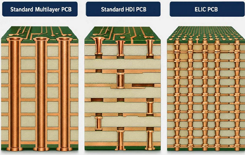
Any layer HDI PCB is a type of high density interconnect board where every layer can interconnect with any other using stacked microvias. Unlike traditional designs with limited via access between select layers, this configuration offers unmatched layout freedom. Engineers use HDI printed circuit board structures when space is tight, but performance can’t be compromised.
These boards use methods such as laser drilling and sequential lamination. The goal is to make interconnects more direct, reducing signal loss and delays. They’re ideal for devices needing high signal integrity in a small footprint. Smartphones, medical instruments, and high-speed communication modules benefit from this approach.
A major advantage lies in compactness. The lack of constraints between layers means denser routing, reduced crosstalk, and better thermal control. The complexity, however, means production is costlier. But the performance tradeoff is often worth it.
In any compact design pushing boundaries, an HDI circuit board with this structure offers engineers the flexibility to execute sophisticated layouts with fewer limitations.
How Is Any Layer HDI PCB Different from Standard HDI PCBs?
The major difference between any layer and standard HDI circuit boards lies in interconnect accessibility. Standard HDI designs allow via connections only between specific layers. In contrast, any layer HDI PCBs permit connections from every layer to every other layer, providing greater flexibility. This structure reduces the length of signal paths, which boosts signal integrity and overall board performance.
Any layer HDI designs also demand a different manufacturing approach. With more microvias and complex stack-ups, the fabrication process becomes more involved. The benefit is that tighter routing and space savings are crucial for next-gen compact devices.
Designers lean toward any layer when working with high-pin-count components or when routing is severely constrained. Any layer helps avoid signal congestion without sacrificing reliability, which is why it’s used in smartphones, miniaturized modules, and high-frequency gear.
The term high density interconnect accurately reflects this design style’s ability to pack features into limited board real estate tightly. The tradeoff is cost, but the technical upside often outweighs it.
Routing Flexibility
Routing becomes simpler with any layer HDI PCBs. Since every layer can connect directly to any other, designers aren’t boxed into fixed via patterns. This freedom helps avoid congestion in dense areas, especially under large chips. Tracks can be kept shorter, which helps maintain signal clarity.
It also makes rerouting easier during late-stage changes. You don’t need extra layers just to complete a connection. That keeps the design efficient and controlled.
Routing flexibility makes the difference for applications where space is tight, like mobile phones or wearables. The high density interconnect layout lets designers hit tight targets without compromise. It’s a strong reason to adopt this technology over standard setups.
Stackup Complexity
Stackup design in any layer HDI PCBs is more involved. Unlike traditional boards with a basic sequence of layers, these boards can have multiple layers, each capable of interconnecting with any other.
Because of this, designers often work with thinner materials and precise lamination steps. The stack must maintain mechanical strength while accommodating several layers of microvias and traces. Signal integrity, heat management, and electrical performance all hinge on how this stack is arranged.
This complexity also affects production timelines and costs. Still, the tradeoff is more efficient use of space and better routing. For high-end electronics, especially HDI printed circuit board applications, it’s a justifiable design choice.
Component Density
More components in less space is the core benefit of any layer HDI PCBs. Since routing is more flexible, designers can place parts closer together. This layout supports high-pin-count chips like processors, memory modules, or FPGAs.
Dense component placement is essential in mobile devices and advanced wearables. It allows more features without increasing the board size. Even with this crowding, signal quality remains high because of shorter interconnect paths.
Using a high density interconnect structure makes it easier to meet EMI and EMC standards as well. Tighter control over signal loops helps reduce noise and interference. It’s an effective solution when board real estate is at a premium.
Manufacturing Process of Any Layer HDI PCBs
Building any layer HDI PCBs involves a detailed and highly controlled process. It starts with the base material and advances through several microvia drilling, plating, and lamination cycles. Each internal layer can connect to any other, so precision at every step matters.
Unlike standard HDI circuit boards, these boards require repeated lamination steps to stack multiple layers. After each layer is added, laser microvias are drilled, cleaned, and plated, making sure of electrical continuity through the stacked structure. Each cycle adds complexity and time, but it’s necessary for the final board’s performance.
Material handling becomes more delicate with thinner cores and tighter tolerances. Even small alignment errors can ruin a whole batch. Manufacturers must use advanced imaging and registration techniques to avoid defects.
Despite the added difficulty, the results are worth it. These boards offer better electrical behavior and space savings. High-density interconnect solutions like this make it possible for devices needing higher functionality in smaller footprints.
Laser Drilling for Microvias
Laser drilling is essential in any layer HDI PCB production. Traditional mechanical drills are too wide for the tiny vias needed here. Instead, lasers cut clean, controlled microvias, usually 50 to 150 microns in diameter.
Each laser pulse must be aligned precisely with internal layer pads. Even slight shifts affect connectivity. Laser drilling’s advantage is that it minimizes board damage and delivers accurate, repeatable results.
Since HDI printed circuit board designs often require multiple stacked microvias, precision is everything. Manufacturers rely on short-pulse or UV lasers as designs grow more compact to deliver clean results on thinner materials. The process is fast, but every via must pass inspection.
Via Filling and Plating
After drilling, microvias must be filled and plated to make sure of strong electrical connections and a flat surface for the next layer. Conductive filling materials, usually copper paste or epoxy with metal particles, are used.
The fill must be void-free. If there’s air trapped inside, it can cause delamination or connection failures later. After filling, electroplating adds copper to connect the vias to the adjacent layers.
In high density interconnect PCBs, these vias are often stacked. That means any weak spot in one layer affects the entire stack. Consistency in plating thickness and coverage is vital. The process might sound straightforward, but the margin for error is tiny.
Sequential Lamination
Sequential lamination involves layering materials step-by-step. For any layer HDI PCBs, this isn’t a one-and-done process. Each new pair of layers must be laminated, drilled, and plated before the next is added.
This builds the structure from the inside out. Every lamination step adds stress, so temperature and pressure must be tightly controlled. Otherwise, warping or misalignment can occur.
Compared to traditional HDI circuit boards, the number of lamination cycles is higher. That’s why this method takes longer and costs more. But it’s what enables full interconnectivity between all layers.
Sequential lamination helps support fine-line routing and dense component layouts without compromising performance.
Ultra-Thin Material Handling
Ultra-thin materials make Any Layer HDI builds possible, but they also introduce handling challenges. These substrates bend easily, making them tricky during drilling, imaging, and lamination. One wrong move and the core warps or tears.
Manufacturers often use vacuum tables and special clamping systems to hold the material flat. Cleanroom environments help avoid particles that could cause shorts or lift the layers. Every step must protect the substrate.
Warping can throw off alignment or affect signal paths in HDI circuit boards. Thin materials improve performance, but they demand extra care. Specialized equipment and experienced technicians are essential, and not every shop can handle this.
Advantages of Any Layer HDI PCBs
Any Layer HDI PCB offers clear benefits for modern electronics. Full layer-to-layer connectivity allows for extremely dense routing, which means designers have more freedom to place components where they’re needed without worrying about via constraints.
By removing the limits of stacked or staggered vias, routing becomes easier. This helps keep the board compact, which is critical for space-constrained products. It also reduces trace length, improving signal speed and integrity.
These boards are often used in applications that need top performance, like HDI printed circuit board solutions for 5G, medical, or aerospace gear. The shorter, cleaner signal paths improve electrical performance, and the tighter structure also benefits heat dissipation.
Though production is more expensive, the final result is a thinner, faster, and more efficient PCB. When reliability and miniaturization matter most, high density interconnect designs like Any Layer HDI stand out. They balance functionality with footprint like few others can.
Unmatched Design Flexibility
Designers love the flexibility that Any Layer HDI brings. Every internal layer can connect to any other layer without relying on stacked microvias in predefined areas, opening up routing possibilities like never before.
This is especially helpful for high density interconnect layouts with fine-pitch components. Tight spacing becomes manageable, and designers can reduce the number of routing layers, saving board space and cost.
Any change in placement doesn’t force a full reroute. Connections are not tied to specific layer stacks, so faster prototyping and easier revisions follow.
With such freedom, meeting electrical requirements without compromising layout is easier. Signal paths stay short and clean.
Supports High-Pin-Count Components
High-pin-count components like FPGAs and ASICs demand more interconnects per square inch. Any Layer HDI PCBs are built for this. They allow direct connections between any internal layer, removing the routing bottlenecks of traditional stacked or staggered vias.
This structure keeps trace lengths short and signal timing consistent. In applications with complex ICs, this becomes critical. It also minimizes the need for fanout routing, freeing space for additional features or simpler ground and power distribution.
HDI printed circuit board assemblies that include BGA packages benefit the most. The routing density around the pins becomes more manageable.
Compact Form Factor
Space constraints often shape electronic product designs. Any Layer HDI PCBs help shrink the board without cutting performance. By enabling connections between all layers, designers can reduce the number of routing layers and the board’s overall size.
This is ideal for wearables, smartphones, and other products where millimeters matter. These boards support finer line widths and tighter spacing, which are important for compact builds.
The high-density interconnect structure makes use of every square inch. Despite the smaller form factor, functionality can remain the same or even improve. Compact doesn’t mean compromised.
Designers achieve thinner, lighter boards without losing flexibility in layout or reliability in performance.
Improved Signal Integrity
Signal integrity matters in high-speed applications. Any Layer HDI PCBs keep signal paths short and direct, reducing signal loss and reflection, especially in high-frequency circuits.
Shorter vias and traces result in fewer impedance mismatches. That means cleaner signal transitions and fewer timing errors. Crosstalk also drops since traces are isolated in tightly controlled layer stacks.
HDI circuit boards using Any Layer architecture are often chosen for RF modules and data transfer devices. They help maintain high data rates and low power noise.
In summary, improved signal integrity is a built-in advantage of this layout style. It’s why engineers choose it for demanding electronics.
Reduced Layer Count
One of the benefits that’s easy to overlook is the chance to reduce total layers. Traditional boards often need extra layers just to manage routing. With Any Layer HDI PCBs, that’s less of a concern.
Because every layer can interconnect directly with any other, designers have more freedom. They don’t need to add intermediate layers just for via paths. That reduces board thickness and potentially cuts costs.
This also makes stackup design more flexible. There’s no strict need to mirror layers or balance routing across sections.
High density interconnect designs simplify what would otherwise be complex layer configurations, thus streamlining the process without limiting electrical performance.
Applications of Any Layer HDI PCBs
Any Layer high density interconnect PCBs serve a wide range of industries that require compact, high-speed, and high-performance electronic systems. Their flexibility and precision make them ideal for applications where space is limited and performance is critical.
Consumer electronics companies support the development of thinner smartphones, wearable devices, as well as smart home gadgets. The miniaturization enabled by HDI circuit boards directly contributes to better portability and functionality.
In medical devices, such as portable monitors or implantable electronics, their tight layout and reduced signal interference are crucial. For 5G and telecommunications, these boards handle high-frequency signals efficiently, making sure of data integrity and lower latency.
Automotive electronics, including advanced driver-assistance systems (ADAS), benefit from improved reliability and thermal performance. In aerospace and defense, Any Layer PCBs provide the needed durability and performance in extreme environments.
The broad adoption of these boards shows how necessary HDI printed circuit board technology has become across many electronic design sectors.
Consumer Electronics
In consumer electronics, compactness and performance go hand in hand. Devices like smartphones, wearables, and tablets use Any Layer HDI PCBs to reduce size without compromising functionality. These boards support fine-pitch components and tight routing.
That makes them ideal for Bluetooth chips, memory, sensors, and processors packed into minimal space. High density interconnect design allows for more complex features in thinner enclosures. Think longer battery life, more storage, or faster processing, all in a smaller shell.
Since consumer electronics thrive on miniaturization, HDI circuit boards keep evolving to support these needs. They enable feature-rich gadgets to fit into pockets and wrists with ease and consistency.
5G and Telecommunications
Speed, frequency, and data rates drive 5G tech. Any Layer HDI PCBs meet the requirements for signal clarity and layout precision in telecom gear. Routers, base stations, and antennas rely on HDI printed circuit board layers to reduce noise and preserve signal timing.
They allow for low-loss routing and consistent impedance. High-speed processors and RF chips can be placed closer together, minimizing delay. With Any Layer access, signals reach their targets faster and cleaner.
High density interconnect techniques keep the board compact while making sure of stability at gigahertz speeds. It’s a solution that helps meet tight tolerance requirements as well as supporting the growing 5G network infrastructure.
Medical Devices
Medical devices demand accuracy, stability, and a compact footprint. Think pacemakers, imaging tools, or patient monitoring systems. These rely heavily on high density interconnect designs for multi-functionality in limited space.
Any Layer HDI PCBs allow designers to manage tight layouts with reliable connections. They also support high-pin-count chips used in signal processing and wireless communication.
Because medical devices often run on battery power, HDI boards help reduce power draw through efficient layout and signal paths. HDI printed circuit board structures also support mechanical stability and EMI control, both important for life-saving equipment.
Their performance and form factor make them a top choice in the healthcare electronics space.
Automotive
Modern vehicles contain dozens of electronic systems, from ADAS to infotainment. These systems need compact, reliable PCBs with high-speed performance. Any Layer HDI PCBs are common in automotive ECUs and driver-assistance modules.
They support small packages and high I/O count chips. Since cars face vibration, heat, and EMI, HDI circuit boards are designed with thermal and structural reliability in mind.
Smaller boards also reduce weight, which is important for EVs and fuel efficiency. In dense dashboards or compact control units, space savings count. High density interconnect layouts keep complexity down and performance up in the high-demand environment of modern vehicles.
Aerospace and Defense
Aerospace and defense systems need rugged PCBs that fit into constrained environments. Radar systems, avionics, and guidance controls all require precision. Any Layer HDI PCBs support this with layered routing and durable construction.
They handle high-pin-count components in tight spaces, often near sensitive equipment. HDI printed circuit board architecture minimizes signal loss, critical for radar and communication systems.
Weight savings are crucial in satellites and aircraft. These boards help reduce weight without cutting functionality. They also resist thermal cycling and vibration better than traditional designs.
High density interconnectlayouts are a great match for mission-critical electronics where performance and size are both a priority.
Design Considerations for Any Layer HDI PCBs
Creating a reliable high density interconnect PCB demands detailed planning and strict adherence to design constraints. Any Layer designs allow interconnects between all layers, increasing flexibility, but also complexity.
Key considerations include material selection, which affects thermal performance, signal transmission, and manufacturability. Engineers must also factor in impedance control, especially for high-speed digital or RF signals. A poorly managed trace can compromise signal integrity.
Microvia design plays a major role in routing efficiency. Via placement, aspect ratio, and type, stacked or staggered, must align with both layout and production capabilities. Thermal management becomes critical as components are densely packed, increasing localized heating.
Layer count optimization balances performance with cost. More layers allow more routing freedom, but can increase fabrication time and expense. Designers must weigh this carefully during planning.
Every decision influences reliability, manufacturability, and overall performance. Incorporating these elements early avoids costly redesigns and ensures the HDI printed circuit board meets both performance and production goals.
Material Selection
Choosing the right material affects everything from signal speed to stability and thermal resistance. Low-loss laminates are popular for Any Layer HDI PCBs. They support high-speed signals and minimize distortion.
The base dielectric must handle high temperatures during lamination and drilling. Resin content, CTE, and Tg rating all matter. For multi-layer HDI circuit boards, a mismatch in material properties can cause delamination or warping.
Copper foil type is another point. Rolled annealed copper performs better for impedance control. Material decisions should also factor in compliance with UL or IPC standards. Making the wrong material choice early can lead to failures during production or use.
Impedance Control
Any Layer HDI PCBs are often used in high-speed applications. Impedance control becomes essential when traces handle fast signals. Differential pairs, controlled impedance lines, and return paths must be designed precisely.
The high density interconnect structure shrinks trace width and spacing. Small deviations in dielectric thickness or copper weight throw off target impedance. That’s why stackup design must include proper simulation.
Dielectric materials should have consistent permittivity (Dk). Routing across multiple layers must maintain symmetrical paths to avoid signal reflection. Even plating thickness and solder mask can affect impedance. Careful planning ensures stable signal transmission in compact HDI designs.
Microvia Design
Microvias are necessary for Any Layer HDI PCBs. They connect different layers with short, precise paths. Their size, shape, and placement directly affect reliability as well as space usage.
Staggered or stacked designs offer flexibility but require exact alignment. Misaligned microvias risk cracking. The depth-to-diameter ratio must stay within limits to prevent plating voids. HDI printed circuit board structures typically use laser-drilled microvias with diameters of 0.1mm or smaller.
Copper filling must be uniform to avoid stress points. Via-in-pad designs save space but demand flat fill for proper soldering. Microvia’s strategy needs to balance performance, manufacturability, and structural strength across the board.
Thermal Management
Compact layouts make heat dissipation harder. Any Layer HDI PCBs require smart thermal planning to prevent hotspots. Designers often use copper pours, thermal vias, or heat spreaders to move heat away from critical parts.
Material choice also plays a role. High-Tg materials resist breakdown at elevated temperatures. Poor heat handling leads to warping, delamination, or early component failure.
Adding too many layers increases thermal resistance. Balanced layer stackups help distribute heat more evenly. In HDI circuit boards, thermal vias under power components transfer heat to inner or outer layers, keeping the board cool even in small enclosures or high-power setups.
Layer Count Optimization
More layers mean more routing space, but also more cost. Any Layer HDI design encourages creativity in reducing layer count while still supporting complex routing. The goal is to do more with fewer layers.
Each layer adds complexity to manufacturing. Sequential lamination steps take time and increase the risk of misalignment. For high density interconnect boards, smart component placement and via strategy can reduce the need for extra layers.
Simulations and constraint-driven routing help find efficient paths. Using blind and buried vias or via-in-pad structures conserves space. An optimized layout saves on production and material costs while keeping signal performance strong.
Challenges in Manufacturing Any Layer HDI PCBs
Making Any Layer HDI PCBs is not easy. Their complex layer structure and tight feature spacing demand extreme precision. Even a small mistake during drilling or lamination can ruin the board. With high density interconnect designs, tolerance margins are slim. Manufacturing yield drops if process control isn’t exact.
Laser drilling microvias requires pinpoint accuracy. Any misalignment affects electrical continuity. Sequential lamination, which builds up layers one at a time, takes longer and costs more. Plus, testing these boards for defects is harder due to their dense layout.
Defects such as delamination, voids in plating, or thermal stress damage can sneak in during fabrication. Keeping up with inspection at each stage is necessary. Manufacturers also need specialized equipment and trained operators. For companies that aren’t set up for HDI, producing these boards can be risky and expensive. Despite these challenges, their benefits keep them in demand.
Cost
Any Layer HDI PCBs are more expensive than traditional designs. The reasons start with their materials and build process. Laser drilling, sequential lamination, and tight tolerances raise production time and complexity.
Also, the HDI printed circuit board typically needs premium substrates to maintain electrical and thermal stability. These materials cost more upfront. Add to that the need for advanced machinery, and costs go even higher.
Volume also plays a role. Small runs drive up unit pricing since setup and calibration are intensive. Unlike standard PCBs, where tooling costs are spread over many boards, HDI boards offer less of that buffer, hence cost planning is extremely important for these builds.
Process Complexity
Manufacturing Any Layer HDI PCBs requires precision across multiple steps. Every via, trace, and pad must align perfectly. The use of laser-drilled microvias and sequential lamination adds layers of risk.
Unlike traditional PCBs, high density interconnect boards demand constant checks and adjustments. Misalignment during lamination or poor plating inside microvias can cause failure. With each lamination cycle, the chance of error increases.
This complexity means fewer manufacturers can handle HDI builds at scale. Specialized equipment, controlled environments, as well as highly trained staff are all necessary. Even small changes in temperature/pressure during processing can cause flaws. Maintaining yield should be a priority.
Testing and Quality Control
Testing Any Layer HDI PCBs is tricky due to their compact features. Traditional inspection methods don’t always catch problems in hidden or buried layers. That’s why quality control must use multiple techniques.
Each HDI circuit board needs electrical testing to confirm proper connectivity. But mechanical defects like plating voids, delamination, or via cracks require more advanced inspection tools.
Manufacturers often use X-ray imaging, cross-section analysis, and AOI systems. These help spot internal faults. Testing protocols must be customized for each stackup and via structure.
Skipping or rushing inspection leads to unreliable boards, especially for mission-critical industries. Consistent quality control is what makes or breaks the entire production process.
Testing and Quality Control for Any Layer HDI PCBs
To make sure that the high density interconnect structures are performing well, you must prioritize testing. Traditional inspections aren’t always reliable. These PCBs demand a specialized approach to catch issues that would otherwise remain hidden..
Manufacturers use a mix of X-ray imaging, impedance testing, and environmental simulations to evaluate durability. Each HDI printed circuit board goes through tailored protocols based on its design and final application. Visual inspection alone isn’t enough.
Some defects, like microvia voids or incomplete plating, don’t show visible signs but can cause intermittent failures. So, automated optical inspection (AOI) and X-ray systems fill that gap.
Thermal cycling is used to check how the board reacts to changes in temperature. Impedance testing confirms that signal paths make sure of integrity at high frequencies. Altogether, this multi-step process makes sure of the reliability of PCBs. This is an important requirement before deployement. If your board is more compact, it just makes the testing phase more important for you.
X-Ray Inspection
X-ray inspection is essential for Any Layer HDI circuit boards. It reveals internal structures that can’t be seen with the naked eye, helping to spot voids, cracks, or misaligned vias early.
Since these PCBs involve stacked microvias and buried layers, internal defects are more common. A surface check wouldn’t catch those. X-ray systems give operators a live view of what’s going on inside the stack-up.
They’re particularly effective for checking via quality, especially plating thickness and continuity. X-ray inspection isn’t optional for applications where reliability matters, like aerospace or medical. It’s a required part of the quality control process. Without it, you’d miss critical faults that could cause functional failure in the field.
Impedance Testing
Impedance testing ensures electrical consistency across the layers of a high density interconnect board. High-speed signals can distort or reflect if the impedance varies unexpectedly.
Controlled impedence comes into play here, as it confirms the characteristic impedance of each trace aligns with design targets. Any changes can cause the signal to degrade, mainly in RF or high-speed digital applications.
During testing, time-domain reflectometry (TDR) is commonly used. It sends a signal through the trace and measures reflections. TDR is accurate, fast, & provides a clear picture of line performance. Manufacturers usually run impedance tests during both prototype and volume production phases to maintain consistent signal quality.
Thermal Cycling
Thermal cycling is vital for checking long-term durability in HDI circuit boards. It subjects the board to repeated heating and cooling cycles. This simulates conditions the product may face over its lifetime.
These cycles reveal weaknesses in solder joints, via reliability, and layer adhesion. Stress from expansion and contraction can cause tiny cracks. Catching these early prevents costly field failures.
Manufacturers typically use thermal cycling as part of reliability testing, especially for aerospace or medical-grade boards. Boards are cycled between low and high extremes, then re-evaluated for defects.
For high density interconnect designs, where stacked microvias are common, thermal cycling highlights issues in hidden layers, where traditional inspections fall short.
Automated Optical Inspection (AOI)
AOI helps detect surface defects on HDI printed circuit boards early in the production line. Cameras scan each layer after etching or component placement.
They compare captured images with the design file. If traces are too thin or solder paste is misaligned, AOI catches it fast. This reduces manual inspection time and improves process yield.
For high density interconnect boards, AOI is even more important. With tighter spacing and smaller components, the margin for error is low.
While AOI doesn’t look inside the board, it’s great for identifying surface-level faults like solder bridges/missing pads. It’s usually one of the first checks after assembly.
Recent Innovations in Any Layer HDI Technology
Any Layer high density interconnect PCB designs keep evolving as manufacturing catches up to increasing demands. With electronic devices shrinking, manufacturers are pushing past traditional limitations of HDI circuit boards.
Smaller microvias and thinner materials are now common, allowing tighter routing and improved signal control. Component integration has seen a shift, too. Embedded passive components and fine-pitch BGAs are being used in HDI printed circuit board applications more frequently.
Automation has also stepped up. AI-driven inspection and process control improve precision and reduce defects. Laser drilling has become even more accurate, with multi-wavelength lasers improving microvia consistency.
Stacking multiple layers using advanced sequential lamination is faster and more reliable, and better materials offer thermal and electrical benefits.
Manufacturers are also experimenting with 3D printing technologies to form internal structures that were previously impossible. These innovations signal how Any Layer HDI is moving toward more complex yet cost-efficient builds.
Smaller Microvias
Smaller microvias are changing how HDI circuit boards are designed. These microvias, less than 75 microns in diameter, allow dense routing without increasing board size.
For a high density interconnect PCB, this means more signal paths in the same area. The reduced size also helps with improved signal integrity and lower crosstalk. However, smaller vias need tighter manufacturing control.
The laser drills used must be more precise, and the plating process must ensure that copper fills these smaller features completely.
Smaller microvias are especially useful in designs using fine-pitch BGAs or stacked die packages. They give designers more layout freedom, without affecting performance or reliability.
Material Advancements
Material innovations are making a visible difference in HDI printed circuit board performance. These improvements support tighter tolerances and better thermal stability.
Resins with lower dielectric constants help reduce signal loss. Manufacturers now have access to laminates specifically made for high density interconnect structures. These materials allow for smaller vias and finer traces.
The shift to high-Tg substrates adds strength under heat cycles. Glass-reinforced epoxies and advanced polyimides are often chosen for demanding environments. Compatibility with laser drilling and plating processes is also a key criterion.
Material reliability impacts yields and field performance alike. Engineers must factor all these aspects early in the design process.
Integrated Components
Engineers usually include more integrated components directly into HDI circuit boards in order to save space as well as improve performance. This includes embedded resistors, capacitors, and sometimes even small ICs. These parts reduce surface clutter, enabling shorter signal paths and better high-speed performance.
Integration is especially useful for mobile, RF, and medical applications where space and noise control are priorities.
With Any Layer HDI designs, routing between embedded components becomes more direct. It also simplifies heat dissipation and reduces electromagnetic interference. However, these benefits must be weighed against increased manufacturing complexity.
Specialized design tools are usually needed to account for tolerances, thermal issues, as well as component interactions.
3D Printing in HDI
3D printing is making inroads into high density interconnect PCB fabrication, especially for early-stage prototyping. It allows for faster iteration and layout experimentation without committing to full production.
Additive manufacturing can build complex HDI layers with embedded vias and conductors in a single process. This technique is particularly promising for small-batch or customized projects.
Certain 3D printers can deposit conductive inks along with insulating materials, forming circuit paths layer by layer. This reduces reliance on traditional etching, drilling, and plating.
However, the material properties & resolution of 3D-printed PCBs still lag behind standard HDI methods. It’s a growing field but not yet a full replacement.
Cost Considerations for Any Layer HDI PCBs
Cost remains a significant factor in producing high density interconnect PCBs, especially Any Layer versions. While the benefits are clear, the advanced design and fabrication steps can drive up expenses quickly.
Prototype costs are often higher due to the need for precision equipment, specialized materials, and multiple manufacturing steps like laser drilling and sequential lamination. Smaller production runs mean higher per-unit costs, especially in early design phases.
Volume can influence pricing. HDI circuit boards become more economical at scale, as setup costs get distributed across larger quantities. However, initial tooling and process validation still impact upfront spending.
Material selection also affects the budget. High-performance laminates, low-loss substrates, and reliable via fill materials can significantly increase costs. Choosing the wrong combination can hurt electrical and thermal performance, leading to higher long-term costs.
Being proactive in cost evaluation during the design stage helps avoid surprises. When budgets are planned smartly, a well-designed HDI printed circuit board delivers performance without unnecessary overspending.
Prototype Costs
Any Layer HDI circuit boards typically come with higher prototyping expenses. This is due to the multiple lamination cycles, laser drilling, and tight process controls needed.
Prototype batches often require custom tooling, which adds to upfront costs. Specialized materials and low-volume runs further increase per-unit pricing.
Still, these costs are expected in exchange for the dense layout and advanced performance delivered by high density interconnect technology.
Engineers must budget accordingly during development phases. Working with a PCB manufacturer familiar with HDI prototyping can avoid mistakes and rework.
Open communication helps in clarifying tolerances, via structures, as well as final stack-up expectations before fabrication begins.
Volume Discounts
While prototyping can be costly, ordering HDI printed circuit board assemblies in higher quantities usually brings some relief. Manufacturers often apply volume-based pricing once orders scale past a certain threshold.
For Any Layer HDI designs, this can significantly reduce the cost per board. Fixed tooling and setup costs are spread across more units.
Additionally, bulk material procurement and process streamlining during large runs result in better margins. These discounts don’t erase the added complexity of high density interconnect builds but make them more manageable.
Engineers should discuss pricing tiers early in the planning process to align output with budget goals.
Material Costs
Materials selected for HDI printed circuit board builds carry weight in final pricing. Standard FR4 laminates won’t perform in dense, high-speed layouts.
Instead, manufacturers rely on high-Tg substrates and low-loss dielectric cores. These materials improve signal integrity and thermal resilience but cost more.
Sourcing ultra-thin cores, specialized prepregs, and laser-compatible coatings drives up expenses. Additionally, tighter copper thickness tolerances and surface finishes like ENIG or OSP raise the bill.
While the material cost itself may seem minor per board, it scales quickly with quantity. Choosing materials suited for high density interconnect applications is extremely important for reliability and functionality.
Future Trends in Any Layer HDI PCBs
The future of high density interconnect PCBs is full of promise as technology demands keep rising. Any Layer designs are expected to become more common across consumer and industrial products due to their compact size and electrical performance.
One trend is the growing integration with advanced packaging. Semiconductor companies are pushing for tighter interconnects between chips and PCBs. This requires tighter pitch designs and better thermal behavior, which Any Layer PCBs offer.
5G expansion is another driver. With the evolution of networkds, devices need to support higher frequencies and bandwidth. HDI circuit boards meet these requirements by reducing signal loss and cross-talk.
The rise of IoT and AI applications will also shape future layouts. Sensors, edge devices, and AI accelerators require small, high-performance substrates, making the HDI printed circuit board an essential building block.
Expect further material innovations, automated inspection tools, and greater adoption in critical systems. These changes will support a more connected and intelligent electronics ecosystem.
Integration with Advanced Packaging
Advanced packaging methods are becoming a key factor in developing compact electronics. To support chiplets, multi-die systems, and system-in-package (SiP) solutions, designers are turning to high density interconnect technologies.
Any Layer HDI printed circuit board configurations simplify interconnections between dies and substrates. This helps improve electrical performance while reducing the space needed on the board.
Features like stacked microvias, reduced pitch, and precise alignment make HDI structures compatible with 2.5D and 3D packaging demands. As chip manufacturers move to smaller nodes, interconnect requirements grow tighter.
HDI and advanced packaging are forming a natural alliance to meet miniaturization without sacrificing signal quality or thermal behavior.
5G Expansion
The growth of 5G is pushing design requirements beyond what traditional PCBs can handle. High density interconnect boards support the frequency, bandwidth, and signal integrity needs of next-generation wireless systems.
In 5G applications, HDI circuit boards help manage signal routing in tight spaces, reduce parasitics, and lower EMI. They’re well-suited for mmWave antennas, baseband modules, and RF front-end systems.
As mobile infrastructure evolves and edge devices increase, board real estate is shrinking. Any Layer HDI layouts offer the flexibility and density required.
Combined with thermal stability and high-frequency performance, they are becoming standard in 5G-enabled devices from smartphones to small cells and base stations.
IoT and AI Applications
IoT and AI devices are getting smarter and smaller. To keep up, engineers are moving toward high density interconnect boards that accommodate sensors, processors, and wireless modules in minimal space.
AI accelerators and edge computing units demand high-speed signaling and efficient heat management, which HDI printed circuit board designs can support.
In wearables, industrial monitors, and home automation products, small board footprints and tight integration are essential.
Any Layer HDI configurations make it easier to route signals, maintain integrity, and stack components without adding layers. With the growth of connected smart devices, HDI’s ability to scale down without losing performance becomes increasingly necessary.
Conclusion
Any Layer high density interconnect PCBs reflect the constant push for smaller, faster, and more capable electronic systems. Their ability to connect any layer to any other layer using stacked microvias sets them apart from traditional PCB structures. These boards enable tighter routing, support for high-pin-count devices, and more improved use of board space.
HDI circuit boards with Any Layer structures will be used more and more what with the growth in demand for advanced electronics. Design teams greatly benefit from improved electrical performance and layout flexibility, while manufacturers continue refining processes to meet tighter tolerances. Although the manufacturing process can be complex and cost-sensitive, the long-term value outweighs these initial challenges, primarily in high-performance applications. Understanding how to properly design, test, and manufacture HDI printed circuit board structures is extremely important in order to stay competitive in high-tech industries. With growing adoption and evolving requirements, Any Layer HDI technology continues to shape the future of PCB engineering.


![Understanding PCB Costs & Pricing [Your Complete Guide]](https://hdicircuitboard.com/wp-content/uploads/elementor/thumbs/Understanding-PCB-Costs-Pricing-Your-Complete-Guide-qzzhe6mcaxuolkux3xalfktgavumi9y1aqfbs9bpv4.webp "Understanding PCB Costs & Pricing [Your Complete Guide]")


