
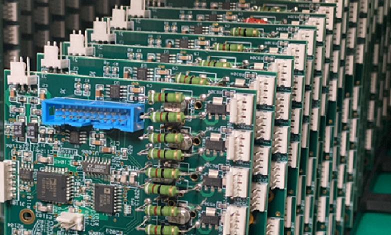
PCB assembly is the manufacturing process that turns a bare printed circuit board into a functional electronic assembly by applying solder paste, placing components, soldering them through reflow, wave, selective, or manual processes, then inspecting and testing the finished PCBA. In production terms, PCB fabrication makes the bare board, while printed circuit board assembly mounts the resistors, capacitors, ICs, connectors, BGAs, transformers, relays, sensors, and other parts that make the circuit work. A reliable PCB assembly process controls solder paste volume, component placement accuracy, reflow profile, through-hole solder fill, BGA X-ray results, ionic cleanliness, functional testing, and final acceptance criteria.
PCB Assembly Basics
PCB vs PCBA
A PCB is the bare board. It contains copper traces, pads, vias, solder mask, silkscreen, surface finish, and drilled holes, but it cannot perform the final product function by itself.
A PCBA is the assembled board. It includes the PCB plus soldered components, inspection records, test results, labels, conformal coating when required, and sometimes firmware loading.
| Term | Meaning | Factory Control |
|---|---|---|
| PCB | Bare printed circuit board | Fabrication, copper, holes, solder mask, finish |
| PCBA | Assembled board with components | SMT, THT, soldering, inspection, testing |
| Circuit card assembly | Industrial term for assembled board | Process control and final acceptance |
| Printed circuit assembly | Another name for PCBA | Component mounting and solder joints |
| PCB fabrication and assembly | Full build from bare board to assembled product | Board fabrication plus assembly flow |
IPC J-STD-001 defines soldering process and material requirements for electronic assemblies, while IPC-A-610 is used for post-assembly acceptance of electronic assemblies. IPC states that these two standards cover assembly process controls, materials, and post-assembly acceptance criteria for the electronics industry.
What PCBA Must Prove
A completed PCB assembly must prove more than electrical continuity. It must show that the board can be built repeatedly with controlled solder joints, correct polarity, stable components, clean residues, and reliable performance under the product’s operating condition.
Production control usually checks:
- Solder paste height and volume
- Component placement offset
- Reflow profile
- Solder joint wetting
- BGA solder voiding
- Through-hole barrel fill
- Connector alignment
- Polarity and orientation
- AOI defect rate
- X-ray result for hidden joints
- ICT or flying probe coverage
- Functional test pass rate
- Final visual acceptance
Key Assembly Methods
Surface Mount Technology
Surface Mount Technology, or SMT, places components directly onto pads on the PCB surface. It is the dominant method for modern PCB assembly because it supports small parts, high component density, automated placement, and fast production.
Typical SMT process ranges:
| SMT Item | Practical Range | Production Meaning |
|---|---|---|
| Stencil thickness | 0.10-0.15 mm common | Controls solder paste volume |
| Fine-pitch stencil | 0.08-0.10 mm by review | Used for QFN, 0.4 mm BGA, micro parts |
| Placement accuracy | ±25-50 microns typical | Supports fine-pitch ICs |
| Reflow peak temperature | 235-250 C lead-free common | Depends on paste and component rating |
| Time above liquidus | 45-90 seconds common | Controls solder wetting |
| SPI threshold | Project-specific, often ±50% volume alarm | Screens paste defects early |
SMT works best for resistors, capacitors, ICs, QFNs, BGAs, LEDs, small connectors, sensors, and high-density electronics.
Through-Hole Technology
Through-Hole Technology, or THT, inserts component leads through plated holes and solders them on the opposite side. It is still used for connectors, transformers, relays, high-current terminals, large electrolytic capacitors, and mechanically stressed parts.
THT soldering methods include:
- Wave soldering for high-volume through-hole parts
- Selective soldering for mixed SMT and THT boards
- Hand soldering for low-volume, rework, or special parts
- Press-fit insertion for some connectors and backplanes
| THT Item | Practical Range | Production Meaning |
|---|---|---|
| Finished hole clearance | Lead diameter + 0.15-0.30 mm | Supports insertion and solder fill |
| Barrel fill target | Often 75% or higher by class and requirement | Ensures mechanical and electrical strength |
| Wave solder pot | About 250-265 C lead-free | Depends on alloy and flux |
| Selective solder nozzle | Project-specific | Protects nearby SMT parts |
| Connector coplanarity | Usually below 0.10-0.20 mm for tight fit | Reduces assembly stress |
THT gives stronger mechanical retention than many SMT joints, but it consumes board area and adds drilling, insertion, and soldering steps.
The Assembly Process
Solder Paste Application
Solder paste application starts the SMT process. A stainless-steel stencil deposits solder paste onto PCB pads. Paste volume must match pad size, component package, stencil thickness, aperture design, and board finish.
Key controls:
- Stencil thickness: usually 0.10-0.15 mm
- Area ratio: often kept above 0.66 for good paste release
- Aperture reduction: common for QFN thermal pads and fine-pitch ICs
- Paste storage: refrigerated, then warmed before use
- Paste life on stencil: controlled by supplier data, humidity, and line time
- SPI: checks height, area, volume, bridging risk, and insufficient paste
Paste problems create most early SMT defects. Insufficient paste can cause opens. Excess paste can cause bridges, solder balls, and BGA voids.
Component Placement
Pick-and-place machines mount components onto solder paste. The machine uses feeders, vision recognition, fiducials, nozzles, placement pressure, and programmed coordinates.
Placement controls:
- Board fiducial recognition before placement
- Feeder verification for part number accuracy
- Nozzle selection by component size and weight
- Polarity and orientation check
- Placement pressure control for fine-pitch parts
- First article inspection before batch run
For 0201 or 01005 passive components, even small paste or placement errors can create tombstoning. For BGA parts, placement looks simple from the top, but hidden solder joints require reflow and X-ray control.
Reflow Soldering
Reflow soldering heats the board through a controlled thermal profile. The solder paste melts, wets the component terminations and PCB pads, then solidifies into solder joints.
Typical lead-free reflow stages:
| Reflow Stage | Typical Range | Purpose |
|---|---|---|
| Preheat ramp | 1-3 C per second | Reduces thermal shock |
| Soak | 150-180 C, 60-120 seconds | Activates flux and stabilizes board temperature |
| Time above liquidus | 45-90 seconds | Forms solder joints |
| Peak temperature | 235-250 C | Melts lead-free solder |
| Cooling rate | 2-4 C per second | Controls grain structure and stress |
Large BGAs, heavy copper boards, metal-core boards, and mixed-mass assemblies need profile tuning. A profile that works for a small sensor board may fail on a thick power assembly.
Inspection and Testing
Inline Inspection
Inspection prevents hidden defects from moving downstream.
Common inspection steps:
- SPI after solder paste printing
- AOI after placement or reflow
- X-ray for BGA, QFN, LGA, via-in-pad, and hidden solder joints
- Visual inspection under IPC-A-610 acceptance criteria
- First article inspection for part number, polarity, and orientation
- Rework verification after repair
IPC-A-610 is a post-assembly acceptance standard used to ensure electronic assemblies meet industry acceptance requirements. IPC J-STD-001 defines soldered assembly process and material requirements.
Electrical Testing
Electrical testing confirms whether the PCBA works as intended.
| Test Method | What It Checks | Best Use |
|---|---|---|
| Flying probe | Opens, shorts, component values | Prototype and low volume |
| ICT | Shorts, opens, resistance, capacitance, diode checks | Medium to high volume |
| Boundary scan | Digital interconnects on scan-capable ICs | Dense boards with limited probe access |
| Functional test | Product-level behavior | Final validation |
| Burn-in | Early-life failure screening | High-reliability products |
| Thermal test | Function at temperature | Industrial, automotive, medical, power electronics |
A board can pass ICT and still fail functional test if firmware, clock startup, RF tuning, power sequencing, or thermal behavior is wrong.
BGA PCB Assembly
How the Process Works
BGA PCB assembly mounts ball grid array packages whose solder balls sit under the component body. Instead of visible side leads, the solder joints are hidden between the package and PCB pads.
BGA process flow:
- Print solder paste on BGA land pads.
- Place the BGA with vision alignment.
- Reflow the assembly using a controlled thermal profile.
- Allow solder balls to collapse and self-align within process limits.
- Inspect hidden joints using X-ray.
- Run electrical and functional testing.
- Rework only with controlled BGA rework equipment when needed.
BGA assembly is common in processors, memory, FPGAs, wireless modules, GPU devices, AI accelerators, microcontrollers, and compact embedded products.
Placement and Reflow
BGA placement requires accurate alignment, stable paste deposit, correct pad design, controlled warpage, and suitable reflow profile.
BGA controls:
| BGA Control | Practical Target | Failure Reduced |
|---|---|---|
| Placement offset | Often below ±50 microns | Ball-to-pad misalignment |
| Package coplanarity | Supplier-specific, usually tight for fine pitch | Opens at package corners |
| Reflow peak | 235-250 C lead-free common | Poor wetting or overheating |
| Void target | Project-specific, often below 25% for many solder joints | Thermal and reliability risk |
| X-ray coverage | BGA and hidden joints | Bridges, voids, opens, head-in-pillow |
| Board warpage | Controlled by stackup and reflow profile | Corner opens and intermittent faults |
BGA rework is expensive and riskier than normal component replacement. The best production strategy is to prevent defects through stencil design, pad design, reflow profiling, and X-ray review.
Inspection
BGA inspection relies on X-ray because the joints are hidden. 2D X-ray can find bridges, large voids, missing balls, and alignment issues. 3D or CT inspection is used when the package is dense, failure mode is unclear, or the product has high reliability requirements.
BGA inspection checks:
- Missing balls
- Solder bridges
- Head-in-pillow defects
- Large voids
- Pad wetting
- Ball collapse uniformity
- Via-in-pad solder wicking
- Corner joint stress
- Rework quality
Advantages of BGA Components
Higher Pin Density
BGA packages provide more I/O in less area than many leaded packages. The ball grid uses the underside of the package, so signal, power, and ground pins can spread across the package body.
Benefits:
- More pins per package area
- Shorter board-level routing
- Better package miniaturization
- Better support for processors, memory, and FPGAs
- Stronger fit for high-density printed circuit assembly
Improved Electrical Performance
BGA packages can improve electrical performance because the interconnect path is shorter than many leaded package styles. Shorter paths reduce parasitic inductance and can improve high-speed signal behavior.
Electrical benefits:
- Shorter connection length
- Lower lead inductance
- Better high-speed capability
- More power and ground balls
- Better decoupling placement options
- Improved support for dense PCBA routing
Better Heat Dissipation
BGA packages often allow improved heat transfer through package balls, thermal pads, PCB copper, and vias. Thermal performance still depends on package design, board stackup, copper area, airflow, and heatsink design.
Thermal controls:
- Thermal via arrays under hot packages
- Copper planes near power devices
- Proper reflow profile
- Package thermal pad design
- Board-level airflow
- Temperature rise measurement under load
Why Specialized Assembly Is Crucial
Process Control
Specialized assembly is crucial when the board uses BGA, QFN, fine-pitch ICs, 0201 passives, heavy connectors, high-current sections, RF circuits, or mixed SMT and THT technology.
A specialized PCBA process should control:
- Stencil design by component type
- Paste type and storage
- SPI before placement
- Placement verification
- Reflow profile by board thermal mass
- X-ray for hidden joints
- AOI library tuning
- ICT or functional test coverage
- Rework limits
- Traceability by lot, panel, and serial number
Quality Control
Quality control must match product risk. A simple LED board and a medical controller should not use the same inspection depth.
| Product Type | Assembly Risk | Extra Control |
|---|---|---|
| Consumer module | Component polarity and solder defects | AOI and functional test |
| Industrial controller | Connector stress and thermal cycling | ICT, thermal test, coating review |
| Medical electronics | Reliability and traceability | Lot control, X-ray, documentation |
| Automotive module | Vibration and temperature | Thermal cycling, conformal coating |
| RF product | Impedance and solder repeatability | RF test and controlled reflow |
| BGA processor board | Hidden solder joints | X-ray and boundary scan |
Two Key Comparisons
SMT vs THT
| Item | SMT | THT |
|---|---|---|
| Component style | Surface-mounted parts | Leads inserted through holes |
| Density | High | Lower |
| Mechanical strength | Good for many parts | Stronger for connectors and heavy parts |
| Production speed | High | Slower |
| Rework difficulty | Moderate to high for fine pitch | Easier for many large parts |
| Best use | ICs, passives, compact electronics | Connectors, terminals, transformers, relays |
PCB Fabrication vs PCB Assembly
| Item | PCB Fabrication | PCB Assembly |
|---|---|---|
| Output | Bare PCB | Functional PCBA |
| Main work | Copper imaging, drilling, plating, solder mask, finish | Paste printing, placement, soldering, inspection, testing |
| Key standards | IPC-2221, IPC-6012 | IPC J-STD-001, IPC-A-610 |
| Main risks | Trace defects, hole plating, impedance drift | Solder defects, wrong parts, hidden BGA faults |
| Inspection | AOI, E-test, microsection, impedance coupon | SPI, AOI, X-ray, ICT, functional test |
| Buyer value | Manufacturable circuit platform | Product-ready electronic assembly |
IPC-2221 supports printed board design requirements, and IPC-6012 covers rigid board qualification and performance. These are important before assembly because poor fabrication quality limits final PCBA yield.
Real Factory Case
Product Background
A customer built a compact industrial data logger with mixed SMT, THT, and one BGA microcontroller. The board was used inside a sealed aluminum enclosure with limited airflow.
| Item | Project Data |
|---|---|
| Board type | Mixed-technology PCBA |
| Layer count | 6 layers |
| Board thickness | 1.6 mm |
| Surface finish | ENIG |
| Smallest passive | 0201 |
| BGA pitch | 0.5 mm |
| THT parts | USB-C shell tabs, relay, terminal block |
| SMT process | Stencil print, SPI, pick-and-place, reflow |
| THT process | Selective soldering and manual touch-up |
| Inspection | SPI, AOI, X-ray, ICT, functional test |
| Test condition | 30-minute thermal run at 55 C |
Production Problem
The first 200-piece pilot build showed several defects:
- 11 boards had BGA void concentration above the internal limit.
- 8 boards had relay pin insufficient solder fill.
- 6 boards failed USB communication after thermal soak.
- 5 boards had 0201 tombstoning near the board edge.
- First-pass yield was 85.0%.
Root cause review found that the stencil aperture under the BGA was too open, the selective solder nozzle angle did not heat one relay pin row evenly, the USB differential pair had good bare-board impedance but poor connector shield soldering, and the edge 0201 parts were affected by local heating imbalance during reflow.
Corrective Actions
The process team changed:
- Reduced BGA paste aperture by 12% in the high-void region.
- Adjusted reflow soak time from 70 seconds to 95 seconds.
- Changed selective solder dwell time from 2.5 seconds to 3.8 seconds on the relay row.
- Added a board edge thermal compensation zone in the reflow profile.
- Increased X-ray sampling on BGA boards from 10% to 100% during pilot.
- Added connector shield solder inspection to AOI criteria.
- Added a 55 C functional test after ICT.
| Metric | First Pilot | Corrected Pilot |
|---|---|---|
| BGA void rejects | 11/200 | 1/300 |
| Relay solder-fill defects | 8/200 | 0/300 |
| USB thermal failures | 6/200 | 0/300 |
| 0201 tombstones | 5/200 | 1/300 |
| First-pass yield | 85.0% | 98.7% |
This case shows why printed circuit board assembly must connect stencil design, reflow profile, selective solder settings, X-ray inspection, and functional testing. The bare PCB was not the main issue. The manufacturing process needed tighter control around package type and board thermal behavior.
Common Assembly Errors
Design Errors
- No fiducials for accurate SMT alignment
- No test pads for ICT or flying probe access
- BGA placed too close to tall connectors
- Fine-pitch ICs placed near board edge without thermal review
- Incorrect footprint for QFN, BGA, or polarized parts
- Insufficient solder mask clearance
- No keepout for selective solder tooling
- Heavy THT parts without mechanical support
Process Errors
- Stencil aperture copied from an old design
- Reflow profile not matched to board mass
- Paste used beyond working life
- Feeder verification skipped
- Selective solder dwell time too short
- X-ray sampling too low for BGA pilot builds
- AOI library not tuned for component height and polarity
- Functional test does not stress power, communication, or thermal load
Documentation Errors
- BOM does not match AVL
- Assembly drawing lacks polarity marks
- Missing centroid file
- Missing solder paste layer review
- Missing test specification
- Missing IPC class requirement
- Missing conformal coating keepout
- Missing rework acceptance criteria
FAQ About PCB Assembly
Question: What is PCB assembly?
Answer: PCB assembly is the process of mounting and soldering electronic components onto a bare printed circuit board to create a working PCBA. The process includes solder paste printing, component placement, reflow soldering, through-hole soldering when needed, inspection, testing, and final quality control.
Question: What is the difference between PCB and PCBA?
Answer: A PCB is the bare printed circuit board with copper traces, pads, holes, solder mask, and surface finish. A PCBA is the assembled board with components soldered onto it. PCBA also includes inspection, testing, labels, firmware when needed, and final acceptance records.
Question: Which assembly method should engineers choose?
Answer: Engineers should choose SMT for high-density components, small passives, ICs, and automated production. THT should be used for connectors, terminals, relays, transformers, and mechanically stressed parts. Many industrial boards use both SMT and THT because density and mechanical strength require different processes.
Question: Why does BGA PCB assembly need X-ray inspection?
Answer: BGA solder joints are hidden under the package, so visual inspection cannot verify all joints. X-ray inspection helps detect solder bridges, missing balls, voids, head-in-pillow defects, alignment issues, and poor collapse. For dense BGA products, X-ray is a key part of reliable PCB assembly.


![Understanding PCB Costs & Pricing [Your Complete Guide]](https://hdicircuitboard.com/wp-content/uploads/elementor/thumbs/Understanding-PCB-Costs-Pricing-Your-Complete-Guide-qzzhe6mcaxuolkux3xalfktgavumi9y1aqfbs9bpv4.webp "Understanding PCB Costs & Pricing [Your Complete Guide]")


