
HDI PCB design guidelines define a strict set of dimension rules, material selections, stackup strategies, and manufacturing constraints aligned with IPC-2226, IPC-2315, and IPC-6016 to enable reliable fabrication of high-density interconnect boards. These guidelines ensure microvia reliability, fine-line yield, impedance control, and signal integrity while supporting miniaturization, fine-pitch components, and high-speed performance in hdi pcb manufacturing.
Learn more about: What is HDI PCB? A Complete Guide for Beginners to High-Density Interconnect
High-Density Interconnect PCB Design Fundamentals
Official HDI Definition (IPC Standards)
High-Density Interconnect PCB design requires compliance with universal industry thresholds:
- Trace width & spacing ≤ 100 μm (4 mil)
- Microvia diameter ≤ 150 μm (6 mil)
- Capture pad size ≤ 400 μm
- Interconnect density ≥ 20 pads/cm²
- Build-up layers with sequential lamination
Core Design Objectives
- Enable 0.3–0.5 mm pitch BGA fan-out without extra layers
- Reduce board size by 30–50% compared to standard PCBs
- Maintain impedance tolerance ±5% for high-speed signals
- Ensure 95%+ manufacturing yield for mass production
- Minimize layer count while preserving electrical performance
HDI PCB Design Rules & Guidelines
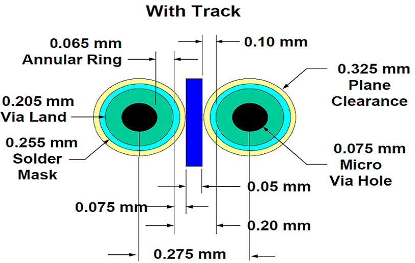
Via Technology
Via Structure
- Microvia diameter: 75–150 μm (laser-drilled only)
- Aspect ratio: ≤ 1:1 (factory best practice ≤ 0.75:1)
- Stacked vias: Max 3 high; require copper filling
- Staggered vias: Offset ≥ 50 μm to prevent shorting
- Skip vias: Aspect ratio ≤ 0.8:1; advanced process only
Via-in-Pad
- Pad size: 0.2–0.3 mm for 0.4 mm pitch components
- Full copper filling required for planarization
- Surface planarity ≤ 5 μm for reliable soldering
- Eliminates fanout routing and reduces trace length by 70%
Trace Width / Spacing
- Minimum line / space: 75/75 μm (3/3 mil) for Type III HDI
- 100/100 μm (4/4 mil) for Type I / Type II HDI
- Impedance trace tolerance: ±10 μm (±0.4 mil)
- 3W rule enforced for high-speed differential pairs
- No 90° corners; 45° or arc bends only (radius ≥ 3× width)
Capture Pads
- Microvia capture pad: ≥ 2.5× via diameter
- Annular ring: ≥ 50 μm for reliable plating
- Anti-pad clearance: ≥ 100 μm around internal vias
- SMD pad size optimized for 0.3–0.5 mm component pitch
Learn more about : Minimum Trace Width, Spacing, and Microvia Size for High Density Interconnect (HDI) PCB Mass Production
Layer Stackup & Material Selection
Stackup Strategy
- Symmetric structure required to control warpage ≤ 0.2 mm/m
- 1+N+1: 1 build-up layer per side (1 lamination cycle)
- 2+N+2: 2 build-up layers per side (2 cycles)
- Core thickness: 0.4–1.0 mm for mechanical stability
- Build-up dielectric thickness: 50–75 μm per layer
Material Selection
- Low-loss materials: Df ≤ 0.009 for high-speed hdi circuit boards
- Standard materials: FR-4 compatible with sequential lamination
- Tg ≥ 170°C for lead-free assembly (260°C reflow)
- Peel strength ≥ 0.8 kgf/cm for reliable microvia adhesion
- Compliance: IPC-4104 for HDI dielectric materials
Layout & Signal Integrity Tips
Placement
- Fine-pitch BGAs placed near stackup center for shortest vias
- High-speed components grouped to minimize trace length
- Keep differential pairs < 200 mil from noisy switching regulators
- Thermal components placed away from RF or precision analog circuits
Routing
- Differential pair length mismatch ≤ 5 mil (≤ 2.5 ps)
- Intra-pair spacing maintained at all times
- No crossing of reference plane gaps or splits
- Orthogonal routing between adjacent signal layers
- Serpentine length matching only with pitch ≥ 5× trace width
Power / Ground
- Solid, continuous reference planes under all high-speed traces
- Power-ground plane pairs spaced ≤ 0.1 mm for high capacitance
- Decoupling capacitors placed ≤ 2 mm from BGA power pins
- 0201 MLCCs preferred for high-density hdi pcb layout
- Ground stitching vias: 1 mm pitch along shield traces
Manufacturing Considerations
Via Filling & Copper Plating
- Full copper filling for stacked and via-in-pad structures
- Plating thickness: ≥ 15 μm uniform coverage
- Void limit: ≤ 2% cross-sectional area (IPC-6012 Class 3)
- Plasma desmear required for microvia adhesion
Sequential Lamination
- 1–4 lamination cycles based on HDI order
- Registration tolerance: ± 30–50 μm layer-to-layer
- Bonding film thickness: 50–75 μm for build-up layers
- Pressure-controlled lamination to prevent resin recession
Thermal & Mechanical Stability
- Thermal shock resistance: 1000 cycles –40°C to 125°C
- Warpage control: ≤ 0.2 mm/m for automated assembly
- Copper weight: 12–35 μm (0.5–1 oz) for fine-line etching
- Surface finish: ENEPIG preferred for fine-pitch HDI boards
Design Rule Check (DRC) Parameters
- Microvia aspect ratio ≤ 1:1
- Trace spacing meets 3W rule for differential pairs
- Capture pad ≥ 2.5× via diameter
- No trace routing over plane gaps or slots
- Length matching constraints satisfied
- Clearance to board edge ≥ 0.5 mm
Learn more about: DFM Tips for HDI Circuit Board: High-Yield Manufacturing Guidelines
Key Comparison Tables
HDI Type vs Design Rules
| HDI Type | Structure | Min Trace | Min Microvia | Lamination Cycles |
|---|---|---|---|---|
| Type I | 1+N+1 | 100 μm | 100–150 μm | 1 |
| Type II | 1+N+1 | 100 μm | 100–150 μm | 1 |
| Type III | 2+N+2 | 75 μm | 75–100 μm | 2 |
| Any-Layer | ALI | 50 μm | 50–75 μm | 4+ |
Stacked vs Staggered Microvias
| Via Type | Space Use | Yield Rate | Plating Risk | Best Use |
|---|---|---|---|---|
| Stacked | Minimal | 91–94% | Medium | Ultra-dense routing |
| Staggered | Moderate | 96–98% | Low | High-reliability systems |
Core Technical Parameters
- Trace width / spacing: 75–100 μm
- Microvia diameter: 75–150 μm
- Aspect ratio: ≤ 1:1
- Dielectric thickness: 50–100 μm
- Impedance tolerance: ±5%
- Registration accuracy: ±30–50 μm
- Warpage limit: ≤ 0.2 mm/m
- Surface planarity: ≤ 5 μm for via-in-pad
Case Study
Project Specifications
- HDI Type: 2+8+2 (Type III)
- Layers: 12 total
- Trace width: 75 μm (3 mil)
- Microvias: 100 μm stacked
- Application: 5G automotive telematics module
- Component: 0.4 mm pitch FPGA
Issues Encountered
- Stacked via registration error ±40 μm out of tolerance
- Microvia voiding in 8% of structures
- Trace etching variation ±15 μm beyond limits
- Board warpage 0.35 mm/m causing assembly failure
Improvements Implemented
- Laser drilling calibration reduced registration to ±25 μm
- Optimized plating profile eliminated voiding
- Etch factor compensation stabilized trace tolerance to ±8 μm
- Symmetric stackup and lamination profile reduced warpage to 0.18 mm/m
- Aspect ratio reduced to 0.75:1 for improved plating
Results
- Manufacturing yield improved from 76% to 95.8%
- Impedance variation controlled to ±4.2%
- Module footprint reduced by 32%
- All parameters meet IPC-2226 and IPC-6012 Class 3
Common Design Errors
- Microvia aspect ratio >1:1 creates plating voids and 10–20% yield loss
- Insufficient capture pad size (<2.5× via diameter) causes connection failures
- Asymmetric stackup leads to warpage >0.3 mm/m and assembly rejection
- Trace width below factory capability results in open circuits and low yield
- Missing via-in-pad filling causes BGA pad dimpling and solder defects
Quality Control & Compliance
Testing Protocols
- Microvia cross-section analysis for void evaluation
- TDR impedance testing per IPC-TM-650
- Automated optical inspection for trace and via uniformity
- Interconnect Stress Testing (IST): 500+ cycles
- Thermal cycling validation: –40°C to 125°C
Standards Compliance
- IPC-2226: HDI PCB design standard
- IPC-2315: Microvia design guidelines
- IPC-6016: High-density substrate performance
- IPC-4104: HDI dielectric qualification
- IPC-6012 Class 3: High-reliability acceptance
FAQ
Q1: What are the most critical HDI PCB design guidelines?
A1: Core rules include microvia aspect ratio ≤1:1, trace width ≥75 μm, symmetric stackup, capture pad ≥2.5× via diameter, and 3W spacing for high-speed signals.
Q2: What is the difference between Type I, Type II, and Type III HDI?
A2: Type I/II use 1+N+1 stackup with 1 lamination cycle. Type III uses 2+N+2 with two cycles, 75 μm traces, and stacked microvias for higher density.
Q3: Why is via-in-pad used in HDI PCB design?
A3: Via-in-pad eliminates fanout routing, enables 0.3–0.5 mm pitch BGA escape, reduces trace length, and improves signal integrity in hdi pcb fabrication.
Q4: What material is recommended for HDI PCB design?
A4: Materials with Tg ≥170°C, compatible with sequential lamination, and peel strength ≥0.8 kgf/cm are required. Low-loss materials are used for high-speed designs.
If you need HDI PCB manufacturing or design support, our engineering team provides free DFM analysis and quotation.
Learn more about: How to Choose HDI PCB Stackup for Your Project


![Understanding PCB Costs & Pricing [Your Complete Guide]](https://hdicircuitboard.com/wp-content/uploads/elementor/thumbs/Understanding-PCB-Costs-Pricing-Your-Complete-Guide-qzzhe6mcaxuolkux3xalfktgavumi9y1aqfbs9bpv4.webp "Understanding PCB Costs & Pricing [Your Complete Guide]")


