
Top global HDI PCB manufacturers deliver high-density interconnect solutions with advanced microvia technology, sequential lamination, fine-line imaging, and controlled impedance to support 56Gbps–224Gbps high-speed systems. This factory‑verified guide profiles key suppliers, quantifies process capabilities, outlines certification frameworks, and provides actionable selection criteria for hdi pcb manufacturing projects ranging from quick‑turn prototypes to high‑volume production.
Learn more about: HDI PCB Design Guidelines
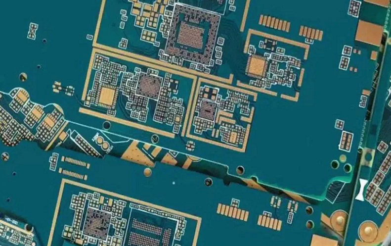
Leading Global HDI PCB Manufacturers
TTM Technologies
TTM Technologies is a global leader in high‑layer‑count HDI and complex sequential lamination structures, serving aerospace, datacom, and automotive markets.
- Layer capability: Up to 40 HDI layers; 68-layer high-layer backplanes
- Microvia size: 75μm minimum; aspect ratio ≤0.75:1
- Line/space: 50μm/50μm inner layers; 75μm/75μm outer layers
- Lamination cycles: Up to 4 sequential cycles
- Certifications: IPC-6012 Class 3, AS9100, IATF 16949, ISO 9001
- Core strength: High-reliability HDI for mission-critical systems
AT&S
AT&S specializes in premium HDI and IC substrate‑like structures for medical, automotive, and mobile applications.
- Stackup structures: 1+N+1, 2+N+2, ELIC any-layer interconnect
- Microvia technology: Stacked filled vias for ultra-high density
- Line/space: 45μm/45μm advanced fine-line capability
- Impedance control: ±5% for high-speed SerDes channels
- Certifications: IPC-6016, ISO 13485, IATF 16949
- Core strength: High-performance HDI for regulated industries
Unimicron Technology Corporation
Unimicron is a high-volume HDI manufacturer focused on consumer electronics, mobile devices, and computing platforms.
- Fine-line capability: 50μm/50μm mass production
- Annual volume: High-output manufacturing for mobile mainboards
- Stackup types: 1+N+1, 2+N+2, and coreless structures
- Surface finishes: ENEPIG, ENIG, OSP, hard gold
- Core strength: Cost-effective high-volume HDI delivery
Compeq Manufacturing Co., Ltd.
Compeq delivers advanced HDI boards with expertise in low-loss materials and high-speed networking applications.
- Material support: Low-loss laminates (Df ≤0.007)
- Layer count: Up to 32 HDI layers
- Back-drilling: Stub length ≤20μm for resonance elimination
- Quality system: IPC-6012 Class 3, ISO 9001, UL
- Core strength: High-speed networking and server HDI boards
Zhen Ding Technology Group
Zhen Ding Technology Group is the world’s largest PCB manufacturer, dominating mobile HDI and substrate-like PCB (SLP) markets.
- Technology: Any-layer ELIC, coreless HDI, mSAP fine-line
- Line/space: Down to 30μm/30μm for ultra-fine designs
- Volume scale: Mass production for flagship mobile devices
- Core strength: Highest-density HDI and SLP for consumer electronics
Benchuang Electronics
Benchuang Electronics is a specialized HDI manufacturer focused on high-mix, quick‑turn production, with deep expertise in 2–7 order HDI structures and high‑reliability applications.
- HDI stackup range: 1+N+1, 2+N+2, 3+N+3, 4+N+4, up to 7-order HDI
- Layer capability: 4–32 standard layers; 56-layer advanced
- Microvia diameter: 75μm minimum; aspect ratio ≤0.75:1
- Line/space: Inner 50μm/50μm; outer 75μm/75μm
- Laser drilling: High-precision blind and buried vias
- Sequential lamination: Up to 4 cycles for stacked via structures
- Materials: High-Tg (≥170°C), low-loss, halogen-free, and high-frequency substrates
- Impedance control: ±5% per IPC-2221; TDR 100% tested
- Quick-turn prototyping: 48-hour rapid samples; 5–10 day standard prototypes
- Certifications: ISO 9001, IATF 16949, UL, RoHS, IPC-6012 Class 3
- Quality control: AOI, X-ray inspection, micro-section, thermal stress testing
- Core strength: Specialized HDI quick‑turn and high‑reliability small‑to‑medium batch production
Meiko Electronics
Meiko Electronics focuses on high‑precision HDI with mature via‑in‑pad and microvia filling processes.
- Via-in-pad: Void-free copper filling; planarity ≤5μm
- Microvia capability: Stacked and staggered structures
- Line/space: 50μm/50μm mass production
- Certifications: IPC-6016, ISO 9001, IATF 16949
- Core strength: High-yield via-in-pad HDI for compact devices
Tripod Technology Corporation
Tripod is a top HDI supplier for memory modules, consumer electronics, and automotive applications.
- HDI expertise: High-density BGA fanout and escape routing
- Layer count: Up to 28 HDI layers
- Production scale: High-volume automotive and mobile HDI
- Core strength: Memory module HDI and automotive interconnects
HDI Manufacturing Core Capabilities
Microvia & Fine-Line Technology
Microvia and fine‑line geometries define routing density and component compatibility in hdi pcb fabrication.
- Minimum microvia diameter: 75μm (laser drilled)
- Aspect ratio: ≤0.75:1 for reliable plating
- Minimum line/space: 50μm/50μm inner; 75μm/75μm outer
- Copper plating: ≥15μm for microvia walls
- Stacked vias: Up to 3 levels with copper filling
Sequential Lamination & Stackup Structures
Sequential lamination builds multi‑layer HDI structures while preserving registration and flatness.
- Lamination cycles: 1–4 cycles supporting 1+N+1 to 4+N+4
- Dielectric thickness: 40μm–100μm per build-up layer
- Registration accuracy: ±25μm layer‑to‑layer
- Warpage control: ≤0.2mm/m for SMT compatibility
- ELIC (Every Layer Interconnect): Any-layer via access for ultra-density
Quick-Turn HDI Prototyping
Rapid prototyping supports fast NPI cycles without compromising quality.
- Prototype lead time: 48 hours–10 days based on complexity
- DFM review: 24-hour engineering turnaround
- Material inventory: Standard and low-loss laminates in stock
- Testing: TDR impedance, AOI, micro-section analysis
Key Manufacturer Comparison Tables
HDI Stackup vs. Manufacturer Strength
| Stackup Type | Speed Range | Leading Manufacturers |
|---|---|---|
| 1+N+1 | ≤28Gbps | Unimicron, Tripod, Benchuang Electronics |
| 2+N+2 | 56–112Gbps | TTM, AT&S, Compeq, Benchuang Electronics |
| ELIC Any-Layer | 224Gbps+ | Zhen Ding, AT&S, Meiko |
Prototype vs. Volume Production Focus
| Supplier Type | Lead Time | Volume | Ideal Application |
|---|---|---|---|
| Quick-Turn Specialist | 2–10 days | Low-Medium | NPI, R&D, Benchuang Electronics |
| High-Volume Maker | 3–6 weeks | High | Consumer Electronics |
| Premium Reliability | 4–8 weeks | Medium-High | Automotive, Aerospace |
Technical Parameters
- Layer count: 4–56 layers
- Board thickness: 0.4mm–7.6mm
- Minimum microvia: 75μm; aspect ratio ≤0.75:1
- Line/space: 50μm/50μm inner; 75μm/75μm outer
- Impedance tolerance: ±5% per IPC-2221
- Registration: ±25μm
- Warpage: ≤0.2mm/m
- Thermal cycling: 1000 cycles −40°C to 125°C
Case Study
Project Overview
- Manufacturer: Benchuang Electronics
- Board type: 12-layer 2+8+2 HDI
- Application: 800G optical transceiver module
- BGA pitch: 0.65mm
- Impedance: 100Ω differential ±5%
Issues Encountered
- Initial microvia aspect ratio 1.1:1 caused 8% plating voids
- Warpage at 0.27mm/m threatened assembly yield
- Insertion loss exceeded 1.1dB at 50GHz
- Trace spacing insufficient for crosstalk targets
Improvements Implemented
- Reduced aspect ratio to 0.7:1
- Implemented fully symmetric stackup
- Switched to ultra-low-loss material (Df ≤0.007)
- Applied 45° routing and expanded clearances
Final Results
- Plating voids <1%
- Warpage stabilized at 0.16mm/m
- Insertion loss ≤0.58dB at 50GHz
- Production yield improved from 79% to 96.3%
- Full compliance with IPC-6012 Class 3
Common Design Errors
- Microvia aspect ratio >0.75:1 causes plating voids and reliability failures.
- Asymmetric stackups induce warpage >0.25mm/m and assembly rejection.
- Insufficient solder mask clearance leads to electrical shorting.
- Reference plane gaps disrupt return paths and increase crosstalk.
- Trace width variation >±10μm breaks impedance targets.
Quality & Compliance Standards
Testing Protocols
- 100% TDR impedance testing for high-speed channels
- Microvia cross-section analysis for void control
- AOI and X-ray inspection for feature integrity
- Thermal stress testing at 288°C ±5°C for 10 seconds
- Insulation resistance ≥10¹²Ω post‑environmental testing
Industry Certifications
- IPC-2221, IPC-2226: HDI design standards
- IPC-6012, IPC-6016: HDI acceptance criteria
- ISO 9001: Quality management
- IATF 16949: Automotive
- ISO 13485: Medical
- AS9100: Aerospace
Considerations for Choosing an HDI Manufacturer
Technical Capability Alignment
- Match microvia, line/space, and stackup to design requirements
- Validate low-loss material and impedance control expertise
- Confirm sequential lamination cycles for complex structures
- Verify quick-turn capacity for prototyping phases
Certification & Quality Validation
- Review industry certifications for target markets
- Inspect reliability test reports and quality records
- Confirm traceability systems for production batches
- Validate IPC Class 2/3 compliance
Frequently Asked Questions
Q1: Which manufacturer is best for quick-turn HDI prototypes?
A1: Benchuang Electronics specializes in rapid 48-hour to 10-day quick‑turn hdi pcb prototypes with full testing and IPC compliance.
Q2: What microvia aspect ratio is safest for HDI manufacturing?
A2: The factory-recommended maximum aspect ratio is ≤0.75:1 to ensure void-free plating and long-term reliability.
Q3: Which stackup is recommended for 112Gbps high-speed designs?
A3: A symmetric 2+N+2 HDI stackup with low-loss materials and staggered microvias delivers optimal performance.
Q4: What impedance tolerance applies to high-speed HDI boards?
A4: Industry and IPC standards require ±5% impedance tolerance for differential channels at 56Gbps and above.
If you need professional HDI PCB design support or quotation, our team provides free DFM check and fast turnaround.


![Understanding PCB Costs & Pricing [Your Complete Guide]](https://hdicircuitboard.com/wp-content/uploads/elementor/thumbs/Understanding-PCB-Costs-Pricing-Your-Complete-Guide-qzzhe6mcaxuolkux3xalfktgavumi9y1aqfbs9bpv4.webp "Understanding PCB Costs & Pricing [Your Complete Guide]")


